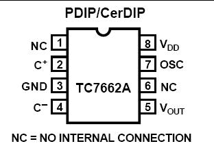
Features: Wide Operating Range ............................. 3V to 18V
Increased Output Current .............................. 40mA
Pin Compatible with ICL7662/SI7661/TC7660/ LTC1044
No External Diodes Required
Low Output Impedance @ IL = 20mA ....... 40 Typ.
No Low-Voltage Terminal Required
CMOS ConstructionPinout Specifications
| Typical Active Output Current (mA) | 40 |
| Output Voltage (V) | Vout = -Vin or Vout = 2Vin |
| Typical Quiescent Current (A) | 190 |
| Input Voltage Range (V) | 3 to 18 |
| Operating Temp. Range (°C) | -45 to 85 |
| Device Description | Inverting or Doubling |
| Typical Active Output Current (mA) |
40 |
| Output Voltage (V) |
Vout = -Vin or Vout = 2Vin |
| Typical Quiescent Current (A) |
190 |
| Input Voltage Range (V) |
3 to 18 |
| Operating Temp. Range (°C) |
-45 to 85 |
| Device Description |
Inverting or Doubling |
Supply Voltage VDD to GND .................................... +18V
Input Voltage (Any Pin) ........................................... (VDD + 0.3) to (VSS 0.3)
Current Into Any Pin .................................................10mA
Operating Temperature Range
C Suffix ........................................................ 0°C to +70°C
I Suffix ....................................................... 25°C to +85°C
E Suffix ...................................................... 40°C to +85°C
M Suffix ..................................................... 55°C to +125°C
Power Dissipation (TA 70°C)
Plastic DIP ..........................................................730mW
CerDIP ...............................................................800mW
SOIC ...........................................................................
Package Thermal Resistance
CPA, EPA JA ...................................................... 140°C/W
IJA, MJA JA ....................................................... 90°C/W
Storage Temperature Range .......................... 65°C to +150°C
Lead Temperature (Soldering, 10 sec) ............ +300°C
ESD Protection..................................................±2000V
Output Short Circuit ........................................ Continuous (at 5.5V Input)DescriptionThe TC7662A is a pin-compatible upgrade to the Industry standard TC7660 charge pump voltage converter. It converts a +3V to +18V input to a corresponding 3V to 18V output using only two low-cost capacitors, eliminating inductors and their associated cost, size and EMI. In addition to a wider power supply input range (3V to 18V versus 1.5V to 10V for the TC7660), the TC7662A can source output currents as high as 40mA. The on-board oscillator operates at a nominal frequency of 12kHz. Operation be-low 10kHz (for lower supply current applications) is also possible by connecting an external capacitor from OSC to ground. The TC7662A directly is recommended for designs requiring greater output current and/or lower input/output voltage drop. It is available in 8-pin PDIP, and CerDIP packages in commercial and extended temperature ranges.
The TC7662A is a pin-compatible upgrade to the Industry standard TC7660 charge pump voltage converter. It converts a +3V to +18V input to a corresponding 3V to 18V output using only two low-cost capacitors, eliminating inductors and their associated cost, size and EMI. In addition to a wider power supply input range (3V to 18V versus 1.5V to 10V for the TC7660), the TC7662A can source output currents as high as 40mA. The on-board oscillator
operates at a nominal frequency of 12kHz. Operation below 10kHz (for lower supply current applications) is also possible by connecting an external capacitor from OSC to ground.
The TC7662A directly is recommended for designs requiring greater output current and/or lower input/output voltage drop. It is available in 8-pin PDIP, and CerDIP packages in commercial and extended temperature ranges.

 TC7662A Data Sheet


