TC7650

Features: • Low Input Offset Voltage: 0.7µV Typ• Low Input Offset Voltage Drift: 0.05µV/°C Max• Low Input Bias Current: 10pA Max• High Impedance Differential CMOS Inputs: 1012Ω• High Open Loop Voltage Gain: 120dB Min.• Low Input Noise Voltage: ...

product image

TC7650 Picture
SeekIC No. : 004514737 Detail

TC7650: Features: • Low Input Offset Voltage: 0.7µV Typ• Low Input Offset Voltage Drift: 0.05µV/°C Max• Low Input Bias Current: 10pA Max• High Impedance Differential CMOS...

floor Price/Ceiling Price

Part Number:
TC7650
Supply Ability:
5000

Price Break

  • Qty
  • 1~5000
  • Unit Price
  • Negotiable
  • Processing time
  • 15 Days
Total Cost: $ 0.00

SeekIC Buyer Protection PLUS - newly updated for 2013!

  • Escrow Protection.
  • Guaranteed refunds.
  • Secure payments.
  • Learn more >>

Month Sales

268 Transactions

Rating

evaluate  (4.8 stars)

Upload time: 2024/12/27

Payment Methods

All payment methods are secure and covered by SeekIC Buyer Protection PLUS.

Notice: When you place an order, your payment is made to SeekIC and not to your seller. SeekIC only pays the seller after confirming you have received your order. We will also never share your payment details with your seller.
Product Details

Description


Features:

• Low Input Offset Voltage: 0.7µV Typ
• Low Input Offset Voltage Drift: 0.05µV/°C Max
• Low Input Bias Current: 10pA Max
• High Impedance Differential CMOS Inputs: 1012
• High Open Loop Voltage Gain: 120dB Min.
• Low Input Noise Voltage: 2.0µVp-p
• High Slew Rate: 2.5V/µsec.
• Low Power Operation: 20mW
• Output Clamp Speeds Recovery Time
• Compensated Internally for Stable Unity Gain Operation
• Direct Replacement for ICL7650
• Available in 8-Pin Plastic DIP and 14-Pin Plastic DIP Packages


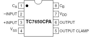
Pinout

  Connection Diagram


Specifications

Total Supply Voltage (VDD to VSS) .......................+18V
Input Voltage .................. (VDD +0.3V) to (VSS 0.3V)
Storage Temperature Range............ -65°C to +150°C
Voltage on Oscillator Control Pins...............VDD to VSS
Duration of Output Short Circuit ................. Indefinite
Current Into Any Pin..........................................10mA
While Operating (Note 3)...........................100µA
Package Power Dissipation (TA 70°C)
8-Pin Plastic DIP ......................................730mW
14-Pin Plastic DIP ....................................800mW
Operating Temperature Range
C Device ...................................... 0°C to +70°C


Parameter Name Value
Temp. Range (°C) 0°C to +70°C
Vos Max (V) 5
# per Package 1
Iq Typical (A) 2000
Iq Max (A) 3500
GBWP (kHz) 2000
Operating Voltage Range (V) 6.5 to 16
Device Description Linear High Precision Op Amps-Chopper Stabilized
PSRR Min (dB) 120
CMRR Min (dB) 120
Vos/Ta (uV/°C) 0.01
Ib (pA) 1.5
Aol (dB) 130
PM (deg) 90
Rail-to-Rail Out


Parameter NameValueTemp. Range (°C)0°C to +70°C Vos Max (V)5# per Package1Iq Typical (A)2000Iq Max (A)3500GBWP (kHz)2000Operating Voltage Range (V)6.5 to 16Device DescriptionLinear High Precision Op Amps-Chopper StabilizedPSRR Min (dB)120CMRR Min (dB)120Vos/Ta (uV/°C)0.01Ib (pA)1.5Aol (dB)130PM (deg)90Rail-to-RailOut


Description

The TC7650 CMOS chopper stabilized operational amplifier practically removes offset voltage error terms from system error calculations. The 5µV maximum VOS specification, for example, represents a 15 times improvement over the industry standard OP07E. The 50nV/°C offset drift specification is over 25 times lower than the OP07E. The increased performance eliminates VOS trim procedures, periodic potentiometer adjustment and the reliability problems caused by damaged trimmers.

The TC7650 performance advantages are achieved without the additional manufacturing complexity and cost incurred with laser or "zener zap" VOS trim techniques.

The TC7650 nulling scheme corrects both DC VOS errors and VOS drift errors with temperature. A nulling amplifier alternately corrects its own VOS errors and the main amplifier VOS error. Offset nulling voltages are stored on two user supplied external capacitors. The capacitors connect to the internal amplifier VOS null points. The main amplifier input signal is never switched. Switching spikes are not present at the TC7650 output.

The 14-pin dual-in-line package (DIP) has an external oscillator input to drive the nulling circuitry for optimum noise performance. Both the 8 and 14-pin DIPs have an output voltage clamp circuit to minimize overload recovery time.


TC7650 CMOS chopper-stabilized operational amplifier practically removes offset voltage error terms from system error calculations. 5V maximum VOS specification, for example, represents a 15 times improvement over the industry-standard OP07E. 50 nV/°C off-set drift specification is over 25 times lower than the OP07E. Increased performance eliminates VOS trim procedures, periodic potentiometer adjustment and the reliability problems caused by damaged trimmers. The TC7650 performance advantages are achieved without the additional manufacturing complexity and cost incurred with laser or "zener zap" VOS trim techniques. The TC7650 nulling scheme corrects both DC VOS errors and VOS drift errors with temperature. A nulling amplifier alternately corrects its own VOS errors and the main amplifier VOS error. Offset nulling voltages are stored on two user-supplied external capacitors. The capacitors connect to the internal amplifier VOS null points. The main amplifier input signal is never switched. Switching spikes are not present at the TC7650 output. The 14-pin dual-in-line package (DIP) has an external oscillator input to drive the nulling circuitry for optimum noise performance. Both the 8 and 14-pin DIPs have an output voltage clamp circuit to minimize overload recovery time.


Customers Who Bought This Item Also Bought

Margin,quality,low-cost products with low minimum orders. Secure your online payments with SeekIC Buyer Protection.
Audio Products
RF and RFID
Power Supplies - Board Mount
Connectors, Interconnects
Memory Cards, Modules
Optoelectronics
View more