TC5002BP

Features: SpecificationsDescriptionThe TC5002BP is designed as decoders to convert BCD code input to the driving signal for 7-segment display element and equipped with NPN transistors as the output buffers enabling direct driving of common cathode type LED. When BI input is set at H level, all t...

product image

TC5002BP Picture
SeekIC No. : 004513813 Detail

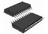
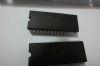
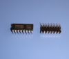
TC5002BP: Features: SpecificationsDescriptionThe TC5002BP is designed as decoders to convert BCD code input to the driving signal for 7-segment display element and equipped with NPN transistors as the output ...

floor Price/Ceiling Price

Part Number:
TC5002BP
Supply Ability:
5000

Price Break

  • Qty
  • 1~5000
  • Unit Price
  • Negotiable
  • Processing time
  • 15 Days
Total Cost: $ 0.00

SeekIC Buyer Protection PLUS - newly updated for 2013!

  • Escrow Protection.
  • Guaranteed refunds.
  • Secure payments.
  • Learn more >>

Month Sales

268 Transactions

Rating

evaluate  (4.8 stars)

Upload time: 2024/7/2

Payment Methods

All payment methods are secure and covered by SeekIC Buyer Protection PLUS.

Notice: When you place an order, your payment is made to SeekIC and not to your seller. SeekIC only pays the seller after confirming you have received your order. We will also never share your payment details with your seller.
Product Details

Description


Features:


Specifications


Description

The TC5002BP is designed as decoders to convert BCD code input to the driving signal for 7-segment display element and equipped with NPN transistors as the output buffers enabling direct driving of common cathode type LED. When BI input is set at "H" level, all the segment outputs are turned "OFF" (not illumination) regardless of other inputs. RBI input of TC5002BP is to turn the output "OFF" and RBO input is to generate "H" level output only for "0" code input and these are used for leading zerc suppress when connected in cascade.

Some absolute maximum ratings of TC5002BP have been concluded into several points as follow. the first one is about its DC supply voltage which would be from Vss-0.5V to Vss+20V. The second one is about its input voltage which would be Vss-0.5V to Vdd+0.5V. The third one is about its output voltage which would be Vss-0.5V to Vdd+0.5V. The fourth one is about its DC input current which would be +/-10mA. The fifth one is about its power dissipation which would be 300mW. The sixth one is about its storage temperature range which would be from -65°C to 150°C. The seventh one is about its lead temperature / time which would be 260°C / 10 sec.

Also some electrical characteristics about TC5002BP. For Vdd=5V the first one is about its high level output voltage (RBO) which would be min 4.95V and typ 5.00V. The second one is about its low level output voltage (RBO) which would be typ 0.00V and max 0.05V. The third one is about its high level output voltage (a - g) which would be min 4.0V and typ 4.5V. The fourth one is about its high level output current (RBO) which would be min -0.16mA. The fifth one is about its low level output current (RBO) which would be min 0.44mA. The sixth one is about its high level output current (a - g) which would be min -20mA. And so on. For more information please contact us.


Customers Who Bought This Item Also Bought

Margin,quality,low-cost products with low minimum orders. Secure your online payments with SeekIC Buyer Protection.
Audio Products
Discrete Semiconductor Products
Optoelectronics
Soldering, Desoldering, Rework Products
Isolators
View more