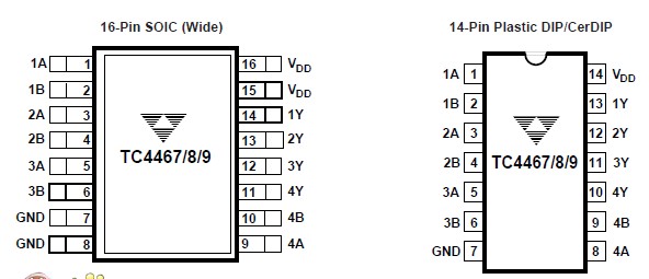
Features: `High Peak Output Current ............................... 1.2A` Wide Operating Range .......................... 4.5 to 18V`Symmetrical Rise and Fall Times ....................25nsec` Short, Equal Delay Times ............................ 75nsec`Latchproof! Withstands 500mA Inductive Kickb...
TC4469: Features: `High Peak Output Current ............................... 1.2A` Wide Operating Range .......................... 4.5 to 18V`Symmetrical Rise and Fall Times ....................25nsec` Short...
SeekIC Buyer Protection PLUS - newly updated for 2013!
268 Transactions
All payment methods are secure and covered by SeekIC Buyer Protection PLUS.
`High Peak Output Current ............................... 1.2A
` Wide Operating Range .......................... 4.5 to 18V
`Symmetrical Rise and Fall Times ....................25nsec
` Short, Equal Delay Times ............................ 75nsec
`Latchproof! Withstands 500mA Inductive Kickback
` 3 Input Logic Choices - AND / NAND / AND + Inv
` 2kV ESD Protection on All Pins
· General-Purpose CMOS Logic Buffer
·Driving All Four MOSFETs in an H-Bridge
· Direct Small Motor Driver
· Relay or Peripheral Drivers
·CCD Driver
· Pin-Switching Network Driver
Parameter Name | Value |
Power | Quad |
Peak Output Current (mA) | 1200 |
Output Resistance (RH/RL)(Max. @ 25°C) | 15/15 |
Max. Supply Voltage (V) | 18 |
Input/Output Delay (td1, td2)1 (ns) | 75/75 |
Configuration | Non-Inverting |
Description | Low-side MOSFET Drivers, 0.5A to 1.2A Peak Output Current |
Operating Temp. Range (°C) | -55 to 125 |
Supply Voltage ......................................................... +20V
Input Voltage ......................... (GND 5V) to (VDD + 0.3V)
Maximum Chip Temperature
Operating ........................................................ +150°C
Storage ............................................. 65° to +150°C
Maximum Lead Temperature
(Soldering, 10 sec) ......................................... +300°C
Operating Ambient Temperature Range
C Device .................................................. 0° to +70°C
E Device ............................................. 40° to +85°C
M Device ........................................... 55° to +125°C
Package Power Dissipation (TA £ 70°C)
14-Pin CerDIP ................................................840mW
14-Pin Plastic DIP ...........................................800mW
16-Pin Wide SOIC ..........................................760mW
Package Thermal Resistance
14-Pin CerDIP RqJ-A .............................. 100°C/W
RqJ-C ................................ 23°C/W
14-Pin Plastic DIP RqJ-A ................................80°C/W
RqJ-C ...................................35°C/W
16-Pin Wide SOIC RqJ-A ................................95°C/W
RqJ-C ...................................28°C/W
*Static-sensitive device. Unused devices must be stored in conductive material. Protect devices from static discharge and static fields. Stresses above those listed under Absolute Maximum Ratings may cause permanent damage to the device. These are stress ratings only and functional operation of the device at these or any other conditions above those indicated in the operational sections of the specifications is not implied. Exposure to Absolute Maximum Rating Conditions for extended periods may affect device reliability.