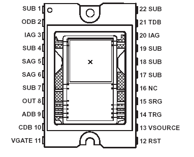
Features: ·High-Resolution, Solid-State Frame-Transfer Image Sensor
· 11.3-mm Image Area Diagonal
· 1000 (H) x 1000 (V) Active Elements
· Up to 30 Frames per Second
· 8-mm Square Pixels
· Low Dark Current
· Advanced Lateral-Overflow-Drain Antiblooming
· Single Pulse Image Area Clear Capability
· Dynamic Range . . . More than 60 dB
· High Sensitivity and Quantum Efficiency
· Nondestructive Charge Detection Through Texas Instruments (TITM) Advanced BCD Node Technology
· High Near-IR and Blue Response
· Solid-State Reliability With No Image Burn-In, Residual Imaging, Image Distortion, Image Lag, or MicrophonicsPinout Specifications
Supply voltage range, VCC: ADB, CDB, TDB, Vgate, Vsource......... SUB to SUB + 15 V
Supply voltage range, VCC; ODB................................................... SUB to SUB + 21 V
Clock voltage range: IAG, SAG, SRG, RST, TRG (see Note 1) ................15 V to 15 V
Operating free-air temperature range, ...........................................TA 10 to 45
Storage temperature range, TSTG....................................................... 30 to 85
Package temperature for guaranteed operation .................................10 to 55
† Stresses beyond those listed under "absolute maximum ratings" may cause permanent damage to the device. These are stress ratings only, and functional operation of the device at these or any other conditions beyond those indicated under "recommended operating conditions" is not implied. Exposure to absolute-maximum-rated conditions for extended periods may affect device reliability.
NOTE 1: Substrate at ground
DescriptionThe TC281 is a frame-transfer charge-coupled-device (CCD) image sensor that provides a very high-resolution image acquisition capability for image-processing applications such as robotic vision, medical X-ray analysis, and metrology. The image sensing area measures 8 mm horizontally and 8 mm vertically; the image-area diagonal measures 11,3 mm and the sensor has 8-mm square pixels. The image area contains 1000 active lines with 1000 active pixels per line. The dark reference signal can be obtained from ten dark reference lines located between the image area and the storage area, 28 dark reference pixels located at the left edge of each horizontal line, and 8 dark reference pixels located at the right edge of each horizontal line.
The storage section of the TC281 contains 1010 lines with 1036 pixels per line. The area is protected from exposure to light by a metal layer. Photoelectric charge that is generated in the image area of the sensor can be transferred into the storage section in less than 110 ms. After the image capture is completed (integration time), the image readout is accomplished by transferring charge, one line at a time, into the serial register located below the storage area. The serial register contains 1036 active pixels and 9 dummy pixels. The maximum serial-register data rate is 40 megapixels per second. If the storage area needs to be cleared of all charge, charge may be quickly transferred across the serial registers into the clearing drain located below the register.
A high performance bulk charge detection (BCD) structure converts charge from each pixel into an output voltage. A low-noise, two-stage, source-follower amplifier further buffers the signal before it is sent to the output pin. A readout rate of 30 frames per second is easily achievable with this device.
The blooming-protection of the sensor is based on an advanced lateral-overflow-drain structure (ALOD). The antiblooming function is activated when a suitable dc bias is applied to the overflow-drain pin. With this type of blooming protection it is also possible to clear the image area of charge completely. This is accomplished by providing a single 10V pulse of at least 1 ms duration to the overflow-drain pin.

 TC281 Data Sheet


