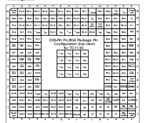
Features: ` Full-duplex asynchronous operating modes 8-bit or 9-bit data frames, LSB first Parity bit generation/checking One or two stop bits Baud rate from 4.6875 MBaud to 1.1 Baud (@ 75 MHz clock` Multiprocessor mode for automatic address/data byte detection` Loop-back capability` Half-duplex 8...
TC1130: Features: ` Full-duplex asynchronous operating modes 8-bit or 9-bit data frames, LSB first Parity bit generation/checking One or two stop bits Baud rate from 4.6875 MBaud to 1.1 Baud (@ 75 MHz clock...
SeekIC Buyer Protection PLUS - newly updated for 2013!
268 Transactions
All payment methods are secure and covered by SeekIC Buyer Protection PLUS.
` Full-duplex asynchronous operating modes
8-bit or 9-bit data frames, LSB first
Parity bit generation/checking
One or two stop bits
Baud rate from 4.6875 MBaud to 1.1 Baud (@ 75 MHz clock
` Multiprocessor mode for automatic address/data byte detection
` Loop-back capability
` Half-duplex 8-bit synchronous operating mode
Baud rate from 9.375 MBaud to 762.9 Baud (@ 75 MHz cloc
` Support for IrDA data transmission up to 115.2 KBaud maximu
` Double buffered transmitter/receiver
` Interrupt generation
On a transmitter buffer empty condition
On a transmit last bit of a frame condition
On a receiver buffer full condition
On an error condition (frame, parity, overrun error)
` FIFO
8 byte receive FIFO (RXFIFO)
8 byte transmit FIFO (TXFIFO)
Independent control of RXFIFO and TXFIFO
9-bit FIFO data width
Programmable Receive/Transmit Interrupt Trigger Level
Receive and Transmit FIFO filling level indication
Overrun error generation
Underflow error generation
` Master and slave mode operation
Full-duplex or half-duplex operation
Automatic pad control possible
` Flexible data format
Programmable number of data bits: 2 to 16 bit
Programmable shift direction: LSB or MSB shift first
Programmable clock polarity: idle low or high state for the shift clock
Programmable clock/data phase: data shift with leading or trailing edge of the sh
clock
` Baud rate generation minimum at 572.2 Baud (@ 75 MHz module clock)
` Interrupt generation
On a transmitter empty condition
On a receiver full condition
On an error condition (receive, phase, baud rate, transmit error)
` Four-pin interface
` Flexible SSC pin configuration
` Up to eight slave select inputs in slave mode
` Up to eight programmable slave select outputs SLSO in master mode
Automatic SLSO generation with programmable timing
Programmable active level and enable control
` 4-stage receive FIFO (RXFIFO) and 4-stage transmit FIFO (TXFIFO)
Independent control of RXFIFO and TXFIFO
2 to 16 bit FIFO data width
Programmable receive/transmit interrupt trigger level
Receive and transmit FIFO filling level indication
Overrun error generation
Underflow error generation
Parameter |
Symbol |
Limit Values |
Unit |
Notes | |
min. |
max. | ||||
Ambient temperature |
TA |
-40 |
85 |
under bias | |
Storage temperature |
TST |
-65 |
150 |
||
Junction temperature |
TJ |
-40 |
125 |
under bias | |
Voltage at 1.5V power supply pins with respect to VSS1) |
VDDC |
0.5 |
1.7 |
V |
|
Voltage at 3.3V power supply pins with respect to VSS2) |
VDDP |
0.5 |
4.0 |
V |
|
Voltage on any pin with respect (VSS2) |
VIN |
0.5 |
4.0 |
V |
|
Voltage on Oscillator Supply pins with respect to ground (VSS ) |
IIN |
10 |
10 |
V |
|
Absolute sum of all input currents during overload condition |
IIN |
|100| |
V |
3) | |
CPU & LMB Bus Frequency |
fsys |
150 |
MHz |
3) | |
FPI Bus Frequency |
f FPI |
100 |
MHz |
||
Power dissipation |
PD |
tbd |
W |
1)Applicable for VDD and VDDOSC.
2)Applicable for VDDP and VDDOSC3 .
The maximum voltage difference must not exceed 4.0V in any case (i.e.Supply Voltage = 4.0V and Input Voltage = -0.5V is not allowed).
3)Restricted life time: TBD
Note:
Stresses above those listed under "Absolute Maximum Ratings" may cause permanent damage to the device. This is a stress rating only and functional operation of the device at these or any other conditions above those indicated in the operational sections of this specification is not implied. Exposure to absolute maximum rating conditions for extended periods may affect device reliability.
During absolute maximum rating overload conditions (VIN > VDD or VIN < VSS ) the voltage on VDD pins with respect to ground (VSS ) must not exceed the value defined by the absolute maximum ratings.