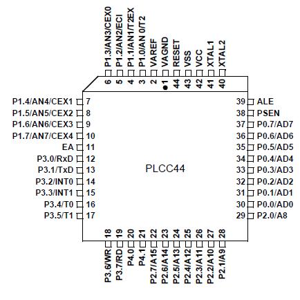
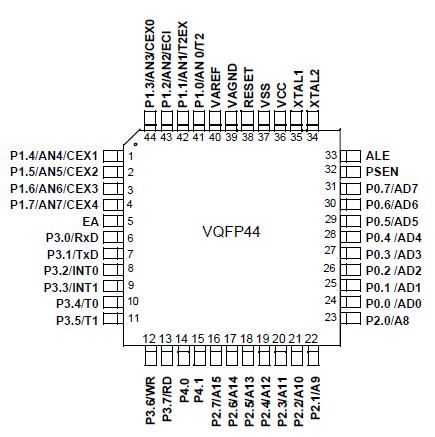
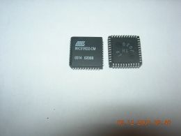
Features: • 80C51 Core Architecture
• 256 Bytes of On-chip RAM
• 1 KB of On-chip XRAM
• 32 KB of On-chip Flash Memory
Data Retention: 10 Years at 85°C
Read/Write Cycle: 10K
• 2 KB of On-chip Flash for Bootloader
• 2 KB of On-chip EEPROM
Read/Write Cycle: 100K
• 14-sources 4-level Interrupts
• Three 16-bit Timers/Counters
• Full Duplex UART Compatible 80C51
• Maximum Crystal Frequency 40 MHz, in X2 Mode, 20 MHz (CPU Core, 20 MHz)
• Five Ports: 32 + 2 Digital I/O Lines
• Five-channel 16-bit PCA with:
PWM (8-bit)
High-speed Output
Timer and Edge Capture
• Double Data Pointer
• 21-bit Watchdog Timer (7 Programmable Bits)
• 10-bit Resolution Analog to Digital Converter (ADC) with 8 Multiplexed Inputs
• On-chip Emulation Logic (Enhanced Hook System)
• Power Saving Modes:
Idle Mode
Power-down Mode
• Power Supply: 3V to 5.5V
• Temperature Range: Industrial (-40° to +85°C)
• Packages: VQFP44, PLCC44ApplicationSoftware can take advantage of the additional data pointers to both increase speed and reduce code size, for example, block operations (copy, compare.) are well served by using one data pointer as a "source" pointer and the other one as a "destination" pointer. Hereafter is an example of block move implementation using the two pointers and coded in assembler. The latest C compiler takes also advantage of this feature by providing enhanced algorithm libraries.
The INC instruction is a short (2 Bytes) and fast (6 machine cycle) way to manipulate the DPS bit in the AUXR1 register. However, note that the INC instruction does not directly force the DPS bit to a particular state, but simply toggles it. In simple routines, such as the block move example, only the fact that DPS is toggled in the proper sequence matters, not its actual value. In other words, the block move routine works the same whether DPS is '0' or '1' on entry.Pinout
 SpecificationsAmbiant Temperature Under Bias:
I = industrial .................................................. -40°C to 85°C
Storage Temperature ............................... -65°C to + 150°C
Voltage on VCC from VSS ....................................-0.5V to + 6V
Voltage on Any Pin from VSS..................... -0.5V to VCC + 0.2V
Power Dissipation ............................................................. 1WDescriptionThe T89C51AC2 is a high performance Flash version of the 80C51 single chip 8-bit microcontrollers. It contains a 32 KB Flash memory block for program and data. The 32 KB Flash memory can be programmed either in parallel mode or in serial mode with the ISP capability or with software. The programming voltage is internally generated from the standard VCC pin.
The T89C51AC2 retains all features of the 80C51 with 256 bytes of internal RAM, a 7- source 4-level interrupt controller and three timer/counters. In addition, the T89C51AC2 has a 10-bit A/D converter, a 2 KB Boot Flash memory, 2 KB EEPROM for data, a Programmable Counter Array, an XRAM of 1024 bytes, a Hardware Watch- Dog Timer, and a more versatile serial channel that facilitates multiprocessor communication (EUART). The fully static design of the T89C51AC2 reduces system power consumption by bringing the clock frequency down to any value, even DC, without loss of data.
The T89C51AC2 has two software-selectable modes of reduced activity and an 8-bit clock prescaler for further reduction in power consumption. In the idle mode the CPU is frozen while the peripherals and the interrupt system are still operating. In the Power-down mode the RAM is saved and all other functions are inoperative.
The added features of the T89C51AC2 make it more powerful for applications that need A/D conversion, pulse width modulation, high speed I/O and counting capabilities such as industrial control, consumer goods, alarms, motor control, among others. While remaining fully compatible with the 80C52, the T8C51AC2 offers a superset of this standard microcontroller. In X2 mode, a maximum external clock rate of 20 MHz reaches a 300 ns cycle time.

 T89C51AC2 Data Sheet

