Transistor Polarity
: N-Channel
Configuration
: Single
Mounting Style
: Through Hole
Maximum Operating Temperature
: + 150 C
Packaging
: Tube
Drain-Source Breakdown Voltage
: 500 V
Continuous Drain Current
: 20 A
Gate-Source Breakdown Voltage
: +/- 30 V
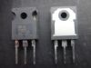
Package / Case
: TO-247
Resistance Drain-Source RDS (on)
: 0.25 Ohms
ApplicationThe MDmesh™ family is very suitable for increasing power density of high voltage converters allowing system miniaturization and higher efficiencies.
Specifications
| Symbol |
Parameter |
Value |
Unit |
| VDS |
Drain-source Voltage (VGS = 0) |
500 |
V |
| VDGR |
Drain- gate Voltage (RGS = 20 k) |
500 |
V |
| VGS |
Gate-Source Voltage |
± 30 |
V |
| ID |
Drain Current (continuous) at Tc = 25 |
20 |
A |
| ID |
Drain Current (continuous) at Tc = 100 |
12.6 |
A |
| IDM(`) |
Drain Current (pulsed) |
80 |
A |
| PTOT |
Total Dissipation at Tc = 25 |
214 |
W |
|
Derating Factor |
1.44 |
W/ |
| dv/dt(1) |
Peak Diode Recovery voltage slope |
15 |
V/ns |
| Tstg |
Storage Temperature |
-65 to 150 |
|
| Tj |
Max. Operating Junction Temperature |
150 |
|
(`) Pulse width limited by safe operating area (1) ISD 14 A, di/dt 200 A/s, VDD V(BR)DSS, Tj TJMAX
DescriptionThe MDmesh™ STW20NM50 is a new revolutionary MOSFET technology that associates the Multiple Drain process with the Company's PowerMESH™ horizontal layout. The resulting product has an outstanding low on-resistance, impressively high dv/dt and excellent avalanche characteristics. The adoption of the Company's proprietary strip technique yields overall dynamic performance that is significantly better than that of similar competition's products.
The STW20NM50 is a kind of N-channel MDmesh™ power MOSFET. The MDmesh™ is a revolutionary MOSFET technology integrating the Multiple Drain process with the PowerMESH™ horizontal layout. It is designed for increasing power density of high voltage converters allowing system miniaturization and higher efficiencies.
There are some features of STW20NM50 as follows: (1) typical RDS(on)=0.20; (2) high dv/dt and avalanche capabilities; (3) 100% avalanche tested; (4) low input capacitance and gate charge; (5) low gate input resistance; (6) tight process control and high manufacturing yields.
What comes next is about the absolute maximum ratings of STW20NM50. (1): VDS (drain-source voltage (VGS=0)) is 500 V; (2): VDGR (drain-gate voltage (RGS=20 k)) is 500 V; (3): VGS (gate-source voltage) is ±30 V; (4): ID (drain current (continuous) at TC=25) is 20 A; (5): ID (drain current (continuous) at TC=100) is 12.6 A; (6): IDM (drain current (pulsed)) is 80 A; (7): PTOT (total dissipation at TC=25) is 214 W; (8): dv/dt (peak diode recovery voltage slope) is 15 V/ns; (9): Tstg (storage temperature range) is from -65 to 150; (10): Tj (maximum operating junction temperature) is 150.
Parameters: | Technical/Catalog Information | STW20NM50 |
| Vendor | STMicroelectronics |
| Category | Discrete Semiconductor Products |
| Mounting Type | Through Hole |
| FET Polarity | N-Channel |
| Drain to Source Voltage (Vdss) | 550V |
| Current - Continuous Drain (Id) @ 25° C | 20A |
| Rds On (Max) @ Id, Vgs | 250 mOhm @ 10A, 10V |
| Input Capacitance (Ciss) @ Vds | 1480pF @ 25V |
| Power - Max | 214W |
| Packaging | Tube |
| Gate Charge (Qg) @ Vgs | 56nC @ 10V |
| Package / Case | TO-247-3 |
| FET Feature | Standard |
| Drawing Number | * |
| Lead Free Status | Lead Free |
| RoHS Status | RoHS Compliant |
| Other Names | STW20NM50
STW20NM50
497 3262 5 ND
49732625ND
497-3262-5
|

 STW20NM50 Data Sheet