SA5512

Features: • Low input bias < ±20nA• Low input offset current < ±20nA• Low input offset voltage <1mV• Low VOS temperature drift 5mV/°C• Low input bias temperature drift 40pA/°C• Low input voltage noise 30nV//Hz• Low supply current 1.5mA/amp• ...

product image

SA5512 Picture
SeekIC No. : 004483692 Detail

SA5512: Features: • Low input bias < ±20nA• Low input offset current < ±20nA• Low input offset voltage <1mV• Low VOS temperature drift 5mV/°C• Low input bias temperatu...

floor Price/Ceiling Price

Part Number:
SA5512
Supply Ability:
5000

Price Break

  • Qty
  • 1~5000
  • Unit Price
  • Negotiable
  • Processing time
  • 15 Days
Total Cost: $ 0.00

SeekIC Buyer Protection PLUS - newly updated for 2013!

  • Escrow Protection.
  • Guaranteed refunds.
  • Secure payments.
  • Learn more >>

Month Sales

268 Transactions

Rating

evaluate  (4.8 stars)

Upload time: 2024/12/25

Payment Methods

All payment methods are secure and covered by SeekIC Buyer Protection PLUS.

Notice: When you place an order, your payment is made to SeekIC and not to your seller. SeekIC only pays the seller after confirming you have received your order. We will also never share your payment details with your seller.
Product Details

Description


Features:

• Low input bias < ±20nA
• Low input offset current < ±20nA
• Low input offset voltage <1mV
• Low VOS temperature drift 5mV/°C
• Low input bias temperature drift 40pA/°C
• Low input voltage noise 30nV//Hz
• Low supply current 1.5mA/amp
• High slew rate 1.0V/ms
• High CMRR 100dB
• High input impedance 100MW
• High PSRR 110dB
• High differential input voltage limit
• No crossover distortion
• Indefinite output short circuit protection
• Internally-compensated for unity gain
• 600W drive capability
• MIL-STD processing available


Application

• AC amplifiers
• RC active filters
• Transducer amplifiers
• DC gain block
• Battery operation
• Instrumentation amplifiers


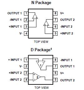
Pinout

  Connection Diagram


Specifications

SYMBOL PARAMETER
RATING
UNIT
VCC Supply voltage
±16
V
PD MAX Maximum power dissipation, TA=25°C (still air)1
  N package
1212
mW
  D package
800
mW
TA Operating ambient temperature range
  NE5512
0 to +70
°C
  SA5512
-40 to +85
°C
  SE5512
-55 to +125
°C
TSTG Storage temperature range
-65 to +150
°C
TSOLD Lead soldering temperature (10sec max)
300
°C
NOTES:
1. The following derating factors should be applied above 25°C
N package at 9.7mW/°C
D package at 6.4mW/°C


Description

The 5512 series of high-performance operational amplifiers provides very good input characteristics. These amplifiers feature low input bias and voltage characteristics such as a 108 op amp with improved CMRR and a high differential input voltage limit achieved through the use of a bias cancellation and PNP input circuits with collector-to-emitter clamping. The output characteristics of 5512 series are like those of a 741 op amp with improved slew rate and drive capability, yet have low supply quiescent current.


Customers Who Bought This Item Also Bought

Margin,quality,low-cost products with low minimum orders. Secure your online payments with SeekIC Buyer Protection.
Test Equipment
Inductors, Coils, Chokes
Line Protection, Backups
RF and RFID
Integrated Circuits (ICs)
Cable Assemblies
View more