PSD834F2

Features: FLASH IN-SYSTEM PROGRAMMABLE (ISP) PERIPHERAL FOR 8-BIT MCUSDUAL BANK FLASH MEMORIESUP TO 2 Mbit OF PRIMARY FLASH MEMORY (8 Uniform Sectors, 32K x8)UP TO 256 Kbit SECONDARY FLASH MEMORY (4 Uniform Sectors)Concurrent operation: READ from one memory while erasing and writing the otherUP TO...

product image

PSD834F2 Picture
SeekIC No. : 004465812 Detail

PSD834F2: Features: FLASH IN-SYSTEM PROGRAMMABLE (ISP) PERIPHERAL FOR 8-BIT MCUSDUAL BANK FLASH MEMORIESUP TO 2 Mbit OF PRIMARY FLASH MEMORY (8 Uniform Sectors, 32K x8)UP TO 256 Kbit SECONDARY FLASH MEMORY (4...

floor Price/Ceiling Price

Part Number:
PSD834F2
Supply Ability:
5000

Price Break

  • Qty
  • 1~5000
  • Unit Price
  • Negotiable
  • Processing time
  • 15 Days
Total Cost: $ 0.00

SeekIC Buyer Protection PLUS - newly updated for 2013!

  • Escrow Protection.
  • Guaranteed refunds.
  • Secure payments.
  • Learn more >>

Month Sales

268 Transactions

Rating

evaluate  (4.8 stars)

Upload time: 2024/11/25

Payment Methods

All payment methods are secure and covered by SeekIC Buyer Protection PLUS.

Notice: When you place an order, your payment is made to SeekIC and not to your seller. SeekIC only pays the seller after confirming you have received your order. We will also never share your payment details with your seller.
Product Details

Description


Features:

FLASH IN-SYSTEM PROGRAMMABLE (ISP) PERIPHERAL FOR 8-BIT MCUS
DUAL BANK FLASH MEMORIES
UP TO 2 Mbit OF PRIMARY FLASH  MEMORY (8 Uniform Sectors, 32K x8)
UP TO 256 Kbit SECONDARY FLASH  MEMORY (4 Uniform Sectors)
Concurrent operation: READ from one memory while erasing and writing the other
UP TO 256 Kbit BATTERY-BACKED SRAM
27 RECONFIGURABLE I/O PORTS
ENHANCED JTAG SERIAL PORT
PLD WITH MACROCELLS
Over 3000 Gates of PLD: CPLD and DPLD
CPLD with 16 Output Macrocells (OMCs) and 24 Input Macrocells (IMCs)
DPLD - user defined internal chip select decoding
27 INDIVIDUALLY CONFIGURABLE I/O PORT PINS
The can be used for the following functions:
MCU I/Os
PLD I/Os
Latched MCU address output
Special function I/Os.
16 of the I/O ports may be configured as open-drain outputs.
IN-SYSTEM PROGRAMMING (ISP) WITH JTAG
Built-in JTAG compliant serial port allows full-chip In-System Programmability
Efficient manufacturing allow easy product testing and programming
Use low cost FlashLINK cable with PC
PAGE REGISTER
Internal page register that can be used to expand the microcontroller address space by a factor of 256
PROGRAMMABLE POWER MANAGEMENT
HIGH ENDURANCE:
100,000 Erase/WRITE Cycles of Flash Memory
1,000 Erase/WRITE Cycles of PLD
15 Year Data Retention
5V±10% SINGLE SUPPLY VOLTAGE
STANDBY CURRENT AS LOW AS 50µA


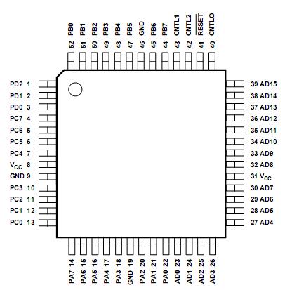
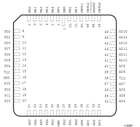
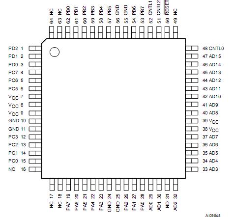
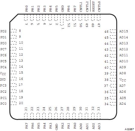
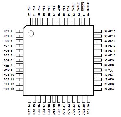
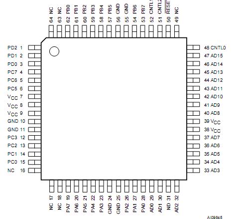
Pinout

  Connection Diagram  Connection Diagram  Connection Diagram


Specifications

Symbol Parameter Min. Max. Unit
TSTG Storage Temperature 65 125 °C
TLEAD Lead Temperature during Soldering (20 seconds max.)1   235 °C
VIO Input and Output Voltage (Q = VOH or Hi-Z) 0.6 7.0 V
VCC Supply Voltage 0.6 7.0 V
VPP Device Programmer Supply Voltage 0.6 14.0 V
VESD Electrostatic Discharge Voltage (Human Body model) 2 2000 2000 V


Description

The PSD834F2 pin connection program:


Customers Who Bought This Item Also Bought

Margin,quality,low-cost products with low minimum orders. Secure your online payments with SeekIC Buyer Protection.
Sensors, Transducers
Optoelectronics
LED Products
Static Control, ESD, Clean Room Products
Fans, Thermal Management
View more