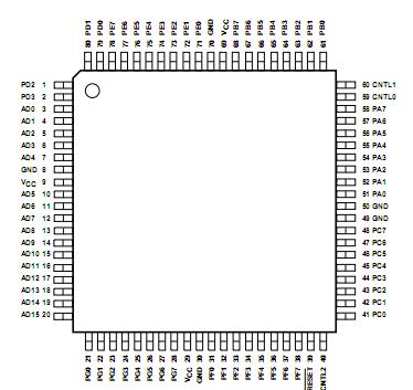
Features: Dual bank Flash memories 8Mbits of Primary Flash Memory (16 uniformsectors, 64Kbyte) 512Kbits of Secondary Flash Memory with 4sectors Concurrent operation: READ from one mem-ory while erasing and writing the other 256Kbits of SRAM (battery-backed) PLD with Macrocells Over 3000 Gates of ...
PSD4256G6V: Features: Dual bank Flash memories 8Mbits of Primary Flash Memory (16 uniformsectors, 64Kbyte) 512Kbits of Secondary Flash Memory with 4sectors Concurrent operation: READ from one mem-ory while era...
SeekIC Buyer Protection PLUS - newly updated for 2013!
268 Transactions
All payment methods are secure and covered by SeekIC Buyer Protection PLUS.
DescriptionThe PSD4135G1V-70J brings In-System-Programmability (ISP) to Flash memory and programma...
Dual bank Flash memories 8Mbits of Primary Flash Memory (16 uniformsectors, 64Kbyte) 512Kbits of Secondary Flash Memory with 4sectors Concurrent operation: READ from one mem-ory while erasing and writing the other
256Kbits of SRAM (battery-backed)
PLD with Macrocells Over 3000 Gates of PLD: CPLD and DPLD CPLD with 16 Output Macrocells (OMCs) and24 Input Macrocells (IMCs) DPLD - user defined internal chip select de-coding
Seven l/O Ports with 52 I/O pins:52 individually configurable I/O port pins thatcan be used for the following functions: MCU I/OsPLD I/Os Latched MCU address output Special function I/Os l/O ports may be configured as open-drainoutputs
In-System Programming (ISP) with JTAG Built-in JTAG compliant serial port allows full-chip In-System Programmability Efficient manufacturing allow easy producttesting and programming Use low cost FlashLINK cable with PC
Page Register Internal page register that can be used to ex-pand the microcontroller address space by afactor of 256
Programmable power management
High Endurance: 100,000 Erase/WRITE Cycles of Flash Mem-ory 1,000 Erase/WRITE Cycles of PLD 15 Year Data Retention
Single Supply Voltage 3V (+20%/10%)
Memory Speed 100ns Flash memory and SRAM access timefor VCC = 3V (+20%/10%) 90ns Flash memory and SRAM access timefor VCC = 3.3V (+/10%)
Symbol |
Parameter |
Min |
Max. |
Unit |
TSTG |
Storage Temperature |
65 |
150 |
°C |
TLEAD |
Lead Temperature during Soldering (20 seconds max.) |
|
235 |
°C |
VIO |
Input and Output Voltage (Q = VOH or Hi-Z) |
0.6 |
40 |
V |
VCC |
Supply Voltage |
0.6 |
40 |
V |
VPP |
Device Programmer Supply Voltage |
0.6 |
135 |
V |
VESD |
Electrostatic Discharge Voltage (Human Body model) |
-2000 |
2000 |
V |
The PSD4256G6V family of memory systems for microcon-trollers (MCUs) brings In-System-Programmability(ISP) to Flash memory and programmable logic.
The result is a simple and flexible solution for em-bedded designs. PSD4256G6V devices combine many ofthe peripheral functions found in MCU based ap-plications.PSD devices integrate an optimized Macrocell log-ic architecture. The Macrocell was created to ad-dress the unique requirements of embeddedystem designs. It allows direct connection be-tween the system address/data bus, and the inter-nal PSD registers, to simplify communicationbetween the MCU and other supporting devices.
The PSD4256G6V family offers two methods to program thePSD Flash memory while the PSD is soldered tothe circuit board: In-System Programming (ISP)via JTAG, and In-Application Programming (IAP).