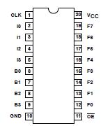
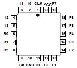
Features: • High-speed version of PLS159
• fMAX = 18MHz 25MHz clock rate
• Field-Programmable (Ni-Cr link)
• 4 dedicated inputs
• 13 control gates
• 32 AND gates
• 21 OR gates
• 45 product terms: 32 logic terms 13 control terms
• 4 bidirectional I/O lines
• 8 bidirectional registers
• J-K, T, or D-type flip-flops
• Power-on reset feature on all flip-flops (Fn = 1)
• Asynchronous Preset/Reset
• Complement Array
• Active-High or -Low outputs
• Programmable OE control
• Positive edge-triggered clock
• Input loading: 100mA (max.)
• Power dissipation: 750mW (typ.)
• TTL compatible
• 3-State outputsApplication• Random sequential logic
• Synchronous up/down counters
• Shift registers
• Bidirectional data buffers
• Timing function generators
• System controllers/synchronizers
• Priority encoder/registersPinout
 Specifications
|
SYMBOL |
PARAMETER |
RATING |
UNIT |
|
MIN. |
MAX. |
|
VCC |
Supply voltage |
|
+7 |
VDC |
|
VIN |
Input voltage |
|
+5.5 |
VDC |
|
VOUT |
Output voltage |
|
+5.5 |
VDC |
|
IIN |
Input currents |
-30 |
+30 |
mA |
|
IOUT |
Output currents |
|
+100 |
mA |
|
TAMB |
Operating free-air temperature range |
0 |
+75 |
|
|
TSTG |
Storage temperature range |
-65 |
+150 |
|
NOTES:
1. Stresses above those listed may cause malfunction or permanent damage to the device. This is a stress rating only. Functional operation at these or any other condition above those indicated in the operational and programming pecification of the device is not implied.
Note
1. Up to 0.3 mm from ceramic.DescriptionThe PLS159A is a 3-State output, registered logic element combining AND/OR gate arrays with clocked J-K flip-flops. These J-K flip-flops are dynamically convertible to D-type via a "fold-back" inverting buffer and control gate FC. PLS159A features 8 registered I/O outputs (F) in conjunction with 4 bidirectional I/O lines (B). These yield variable I/O gate and register configurations via control gates (D, L) ranging from 16 inputs to 12 outputs.
The AND/OR arrays PLS159A consist of 32 logic AND gates, 13 control AND gates, and 21 OR gates with fusible link connections for programming I/O polarity and direction. All AND gates are linked to 4 inputs (I), bidirectional I/O lines (B), internal flip-flop outputs (Q), and Complement Array output (C). The Complement Array consists of a NOR gate optionally linked to all AND gates for generating and propagating complementary AND terms.
On-chip T/C buffers couple either True (I, B, Q) or Complement (I, B, Q, C) input polarities to all AND gates, whose outputs can be optionally linked to all OR gates. Any of the 32 AND gates can drive bidirectional I/O lines (B), whose output polarity is individually programmable through a set of Ex-OR gates for implementing AND-OR or AND-NOR logic functions. Similarly, any of the 32 AND gates can drive the J-K inputs of all flip-flops. There are 4 AND gates for the Asynchronous Preset/Reset functions.
All flip-flops PLS159A are positive edge-triggered and can be used as input, output or I/O (for interfacing with a bidirectional data bus) in conjunction with load control gates (L), steering inputs (I), (B), (Q) and programmable output select lines (E).
The PLS159A is field-programmable, enabling the user to quickly generate custom patterns using standard programming equipment.

 PLS159A Data Sheet


