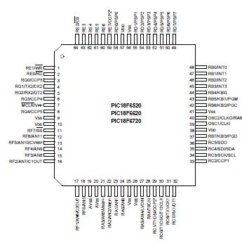
Features: • High current sink/source 25 mA/25 mA
• Four external interrupt pins
• Timer0 module: 8-bit/16-bit timer/counter
• Timer1 module: 16-bit timer/counter
• Timer2 module: 8-bit timer/counter
• Timer3 module: 16-bit timer/counter
• Timer4 module: 8-bit timer/counter
• Secondary oscillator clock option - Timer1/Timer3
• Five Capture/Compare/PWM (CCP) modules:
- Capture is 16-bit, max. resolution 6.25 ns (TCY/16)
- Compare is 16-bit, max. resolution 100 ns (TCY)
- PWM output: PWM resolution is 1 - to 10-bit
• Master Synchronous Serial Port (MSSP) module ith two modes of operation:
- 3-wire SPI™ (supports all 4 SPI modes)
- I2C™ Master and Slave mode
• Two Addressable USART modules:
- Supports RS-485 and RS-232
• Parallel Slave Port (PSP) module
• 10-bit, up to 16-channel Analog-to-Digital onverter (A/D):
- Conversion available during SLEEP
• Programmable 16-level Low Voltage Detection LVD) module:
- Supports interrupt on Low Voltage Detection
• Programmable Brown-out Reset (PBOR)
• Dual analog comparators:
- Programmable input/output configuration
• 100,000 erase/write cycle Enhanced FLASH rogram memory typical
• 1,000,000 erase/write cycle Data EEPROM emory typical
• 1 second programming time
• FLASH/Data EEPROM Retention: > 40 years
• Self-reprogrammable under software control
• Power-on Reset (POR), Power-up Timer (PWRT) nd Oscillator Start-up Timer (OST)
• Watchdog Timer (WDT) with its own On-Chip C Oscillator for reliable operation
• Programmable code protection
• Power Saving SLEEP mode
• Selectable oscillator options including:
- 4X Phase Lock Loop (of primary oscillator)
- Secondary Oscillator (32 kHz) clock input
• In-Circuit Serial Programming™ (ICSP™) via wo pins
• MPLAB® In-Circuit Debug (ICD) via two pinsPinout Specifications
Ambient temperature under bias......................................................................................................-55°C to +125°C
Storage temperature ...................................................................................................................... -65°C to +150°C
Voltage on any pin with respect to VSS (except VDD, MCLR, and RA4) ......................................... -0.3V to (VDD + 0.3V)
Voltage on VDD with respect to VSS ....................................................................................................... -0.3V to +5.5V
Voltage on MCLR with respect to VSS (Note 2) ....................................................................................... 0V to +13.25V
Voltage on RA4 with respect to Vss .......................................................................................................... 0V to +12.0V
Total power dissipation (Note 1) ............................................................................................................................1.0W
Maximum current out of VSS pin ..........................................................................................................................300 mA
Maximum current into VDD pin .............................................................................................................................250 mA
Input clamp current, IIK (VI < 0 or VI > VDD)...................................................................................................... ±20 mA
Output clamp current, IOK (VO < 0 or VO > VDD) ................................................................................................ ±20 mA
Maximum output current sunk by any I/O pin.........................................................................................................25 mA
Maximum output current sourced by any I/O pin ...................................................................................................25 mA
Maximum current sunk by all ports .......................................................................................................................200 mA
Maximum current sourced by all ports ..................................................................................................................200 mA
Note 1: Power dissipation is calculated as follows:Pdis = VDD x {IDD - IOH} + {(VDD-VOH) x IOH} + (VOl x IOL)
2: Voltage spikes below VSS at the MCLR/VPP pin, inducing currents greater than 80 mA, may cause latchup.Thus, a series resistor of 50-100 should be used when applying a "low" level to the MCLR/VPP pin, ratherthan pulling this pin directly to VSS.
† NOTICE: Stresses above those listed under "Absolute Maximum Ratings" may cause permanent damage to the
device. This is a stress rating only and functional operation of the device at those or any other conditions above those
indicated in the operation listings of this specification is not implied. Exposure to maximum rating conditions for
extended periods may affect device reliability.
DescriptionThis document contains device specific information for he following PIC18FXX20 series:
• PIC18F6520 • PIC18F8520
• PIC18F6620 • PIC18F8620
• PIC18F6720 • PIC18F8720
This family offers the advantages of all PIC18FXX20 microcontrollers namely, high computational performance t an economical price - with the addition of igh-endurance Enhanced FLASH program memory. he PIC18FXX20 family also provides an enhanced ange of program memory options and versatile analog eatures that make it ideal for complex, high erformance applications.

 PIC18FXX20 Data Sheet


