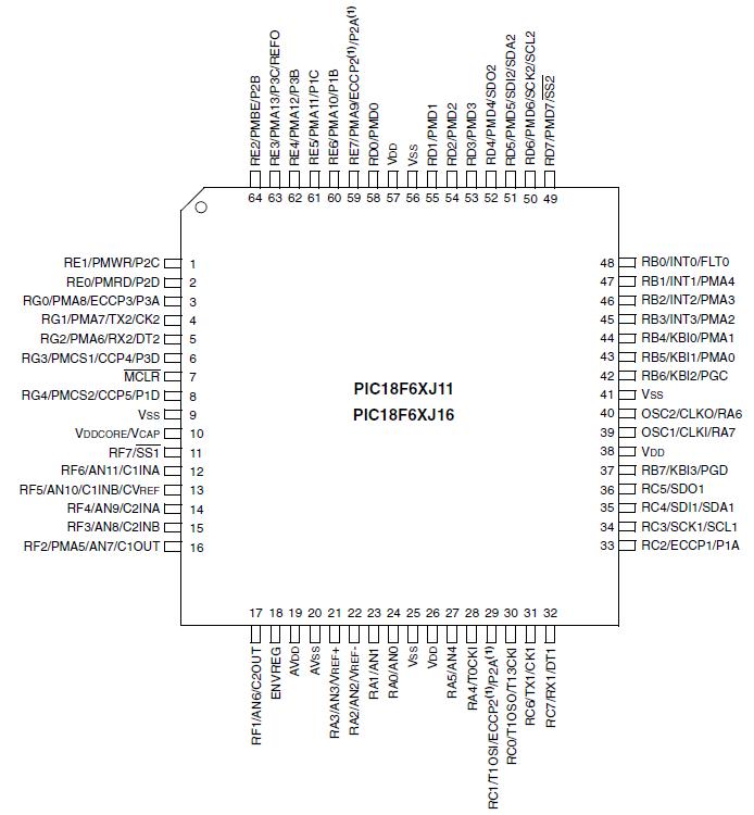
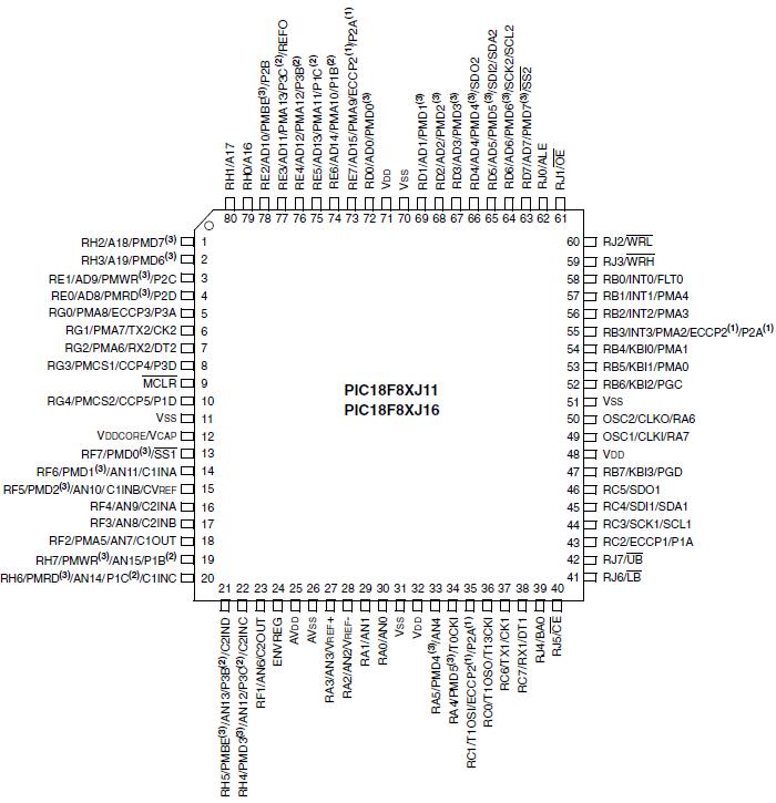
Features: • Low-Power, High-Speed CMOS Flash Technology
• C Compiler Optimized Architecture for Re-Entrant Code
• Power Management Features:
- Run: CPU on, peripherals on
- Idle: CPU off, peripherals on
- Sleep: CPU off, peripherals off
• Priority Levels for Interrupts
• Self-Programmable under Software Control
• 8 x 8 Single-Cycle Hardware Multiplier
• Extended Watchdog Timer (WDT):
- Programmable period from 4 ms to 131s
• Single-Supply In-Circuit Serial Programming™ (ICSP™) via Two Pins
• In-Circuit Debug (ICD) with 3 Breakpoints via Two Pins
• Operating Voltage Range of 2.0V to 3.6V
• 5.5V Tolerant Inputs (digital only pins)
• On-Chip 2.5V Regulator
• Flash Program Memory of 10000 Erase/Write Cycles and 20-Year Data RetentionPinout
 Specifications
| Program Memory Type |
Flash |
| Program Memory (KB) |
128 |
| CPU Speed (MIPS) |
12 |
| RAM Bytes |
3,904 |
| Digital Communication Peripherals |
2-A/E/USART, 2-MSSP(SPI/I2C) |
| Capture/Compare/PWM Peripherals |
2 CCP, 3 ECCP |
| Timers |
2 x 8-bit, 3 x 16-bit |
| ADC |
12 ch, 10-bit |
| Comparators |
2 |
| Temperature Range (C) |
-40 to 85 |
| Operating Voltage Range (V) |
2 to 3.6 |
| Pin Count |
80 |
Ambient temperature under bias......................................................................................................................................-40°C to +100°C
Storage temperature ....................................................................................................................................................... -65°C to +150°C
Voltage on any digital only input pin or MCLR with respect to VSS(except VDD) ............................................................... -0.3V to 6.0V
Voltage on any combined digital and analog pin with respect to VSS................................................................................ -0.3V to (VDD+ 0.3V)
Voltage on VDDCORE with respect to VSS........................................................................................................................... -0.3V to 2.75V
Voltage on VDD with respect to VSS................................................................................................................................... -0.3V to 4.0V
Total power dissipation (Note 1) ...................................................................................................................................... 1.0W
Maximum current out of VSS pin ........................................................................................................................................ 300 mA
Maximum current into VDD pin ........................................................................................................................................... 250 mA
Input clamp current, IIK (VI < 0 or VI > VDD) (Note 2)........................................................................................................ ±0 mA
Output clamp current, IOK (VO < 0 or VO > VDD) (Note 2) ................................................................................................. ±0 mA
Maximum output current sunk by any PORTB and PORTC I/O pins..................................................................................... 25 mA
Maximum output current sunk by any PORTD, PORTE and PORTJ I/O pins ......................................................................... 8 mA
Maximum output current sunk by any PORTA, PORTF, PORTG and PORTH I/O pins............................................................. 2 mA
Maximum output current sourced by any PORTB and PORTC I/O pins................................................................................. 25 mA
Maximum output current sourced by any PORTD, PORTE and PORTJ I/O pins...................................................................... 8 mA
Maximum output current sourced by any PORTA, PORTF, PORTG and PORTH I/O pins ........................................................ 2 mA
Maximum current sunk by all ports combined...................................................................................................................... 200 mA
Maximum current sourced by all ports combined................................................................................................................. 200 mA
Note
1: Power dissipation is calculated as follows: Pdis = VDD x {IDD IOH} + {(VDD VOH) x IOH} + (VOL x IOL) + (VTPOUT x ITPOUT)
2: No clamping diodes are present.
DescriptionPIC18F87J11 is Ideal for 3V applications that are cost senstitive, requiring flexible serial communication with four serial ports: double synchronous serial ports (I2C? and SPI?) and double asynchronous serial ports. Large amounts of Flash program memory make it ideal for instrumentation panels, TCP/IP enabled embedded applications as well as metering, industrial control and monitoring applications. The PIC18F87J11 is an enhancement to the PIC18F87J10 family, including an internal 8MHz oscillator, lower power and improved EEPROM emulation via word Flash write capabilities.

 PIC18F87J11 Data Sheet


