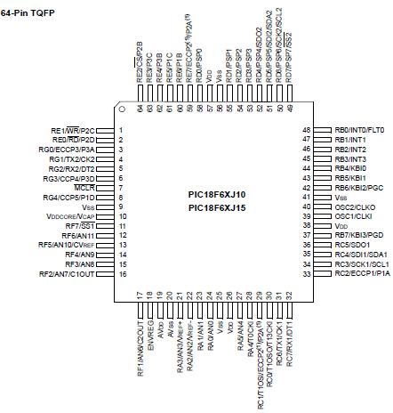
Features: • Operating voltage range: 2.0V to 3.6V
• 5.5V tolerant input (digital pins only)
• On-chip 2.5V regulator
• Low-power, high-speed CMOS Flash technology
• C compiler optimized architecture:
- Optional extended instruction set designed to optimize re-entrant code
• Priority levels for interrupts
• 8 x 8 Single-Cycle Hardware Multiplier
• Extended Watchdog Timer (WDT):
- Programmable period from 4 ms to 131s
• Single-Supply In-Circuit Serial Programming™ (ICSP™) via two pins
• In-Circuit Debug (ICD) with three Break points via two pins
• Power-Managed modes:
- Run: CPU on, peripherals on
- Idle: CPU off, peripherals on
- Sleep: CPU off, peripherals offPinout Specifications
| Program Memory Type |
Flash |
| Program Memory (KB) |
96 |
| CPU Speed (MIPS) |
10 |
| RAM Bytes |
3,936 |
| Digital Communication Peripherals |
2-A/E/USART, 2-MSSP(SPI/I2C) |
| Capture/Compare/PWM Peripherals |
2 CCP, 3 ECCP |
| Timers |
2 x 8-bit, 3 x 16-bit |
| ADC |
11 ch, 10-bit |
| Comparators |
2 |
| Temperature Range (C) |
-40 to 85 |
| Operating Voltage Range (V) |
2 to 3.6 |
| Pin Count |
64 |
Ambient temperature under bias........................................-40°C to +125°C
Storage temperature ........................................................ -65°C to +150°C
Voltage on any digital-only I/O pin with respect to VSS (except VDD and MCLR) .... -0.3V to 5.5V
Voltage on any combined digital and analog pin with respect to VSS (except VDD and MCLR).... -0.3V to (VDD + 0.3V)
Voltage on VDDCORE with respect to VSS................................ -0.3V to 2.75V
Voltage on VDD with respect to VSS ......................................... -0.3V to 3.6V
Voltage onMCLR with respect to VSS (Note 2) ............................. 0V to 3.6V
Total power dissipation (Note 1) ............................................................1.0W
Maximum current out of VSS pin .........................................................300 mA
Maximum current into VDD pin ............................................................250 mA
Input clamp current, IIK (VI < 0 or VI > VDD)..................................... ±20 mA
Output clamp current, IOK (VO < 0 or VO > VDD) .............................. ±20 mA
Maximum output current sunk by PORTB and PORTC I/O pins.................25 mA
Maximum output current sunk by PORTD, PORTE and PORTJ I/O pins .......8 mA
Maximum output current sunk by PORTA, PORTF, PORTG and PORTH I/O pins .......2 mA
Maximum output current sourced by PORTB and PORTC I/O pins .........................25 mA
Maximum output current sourced by PORTD, PORTE and PORTJ I/O pins.................8 mA
Maximum output current sourced by PORTA, PORTF, PORTG and PORTH I/O pins ...2 mA
Maximum current sunk by all ports .........................................................200 mA
Maximum current sourced by all ports .....................................................200 mA
Note 1: Power dissipation is calculated as follows:
Pdis = VDD x {IDD IOH} + {(VDD VOH) x IOH} + (VOL x IOL)
2: Voltage spikes below VSS at the MCLR pin, inducing currents greater than 80 mA, may cause latch-up.Thus, a series resistor of 50-100 should be used when applying a "low" level to theMCLR pin, rather than pulling this pin directly to VSS.
DescriptionIdeal for cost sensitive applications that benefit from the availability of four serial ports: two synchronous serial ports (I2C? and SPI?) and two asynchronous (LIN capable) serial ports. Large amounts of Flash program memory and RAM make PIC18F66J15 ideal for instrumentation panels, TCP/IP enabled embedded applications as well as metering, industrial control and monitoring applications. While operating up to 40 MHz at 3V, this PIC18F66J15 general purpose devices targets cost sensitive designs with 1k Flash endurance, emulated EEPROM, and external crystal or clock source.

 PIC18F66J15 Data Sheet


