Features: • High current sink/source 25 mA/25 mA
• Four external interrupt pins
• Timer0 module: 8-bit/16-bit timer/counter
• Timer1 module: 16-bit timer/counter
• Timer2 module: 8-bit timer/counter
• Timer3 module: 16-bit timer/counter
• Secondary oscillator clock option Timer1/Timer3
• One Capture/Compare/PWM (CCP) module:
- Capture is 16-bit, max. resolution 6.25 ns TCY/16)
- Compare is 16-bit, max. resolution 100 ns (TCY)
- PWM output: PWM resolution is 1 to 10-bit
• Enhanced Capture/Compare/PWM (ECCP) module:
- Same Capture/Compare features as CCP
- One, two or four PWM outputs
- Selectable polarity
- Programmable dead time
- Auto-shutdown on external event
- Auto-restart
• Master Synchronous Serial Port (MSSP) module ith two modes of operation:
- 3-wire SPI™ (supports all 4 SPI modes)
- I2C™ Master and Slave mode
• Enhanced Addressable USART module:
- Supports RS-232, RS-485 and LIN 1.2
- Programmable wake-up on Start bit
- Auto-baud detect
• Parallel Slave Port (PSP) module
• Up to 16-channel, 10-bit Analog-to-DigitalConverter module (A/D) with:
- Fast sampling rate
- Programmable acquisition time
- Conversion available during Sleep
• Programmable 16-level Low-Voltage Detection(LVD) module:
- Supports interrupt on Low-Voltage Detection
• Programmable Brown-out Reset (BOR)
• Dual analog comparators:
- Programmable input/output configuration
• Message bit rates up to 1 Mbps
• Conforms to CAN 2.0B ACTIVE Specification
• Fully backward compatible with PIC18XXX8 CANmodules
• Three modes of operation:
- Legacy, Enhanced Legacy, FIFO
• Three dedicated transmit buffers with prioritization
• Two dedicated receive buffers
• Six programmable receive/transmit buffers
• Three full 29-bit acceptance masks
• 16 full 29-bit acceptance filters with dynamic association
• DeviceNet™ data byte filter support
• Automatic remote frame handling
• Advanced Error Management features
• 100,000 erase/write cycle Enhanced Flashprogram memory typical
• 1,000,000 erase/write cycle Data EEPROMmemory typical
• 1-second programming time
• Flash/Data EEPROM Retention: > 40 years
• Self-reprogrammable under software control
• Power-on Reset (POR), Power-up Timer (PWRT)and Oscillator Start-up Timer (OST)
• Watchdog Timer (WDT) with its own On-ChipRC Oscillator
• Programmable code protection
• Power saving Sleep mode
• Selectable oscillator options including:
- Software enabled 4x Phase Lock Loop (ofprimary oscillator)
- Secondary Oscillator (32 kHz) clock input
• In-Circuit Serial Programming™ (ICSP™) via two pins
• MPLAB® In-Circuit Debug (ICD) via two pinsPinout Specifications
| Program Memory Type |
Flash |
| Program Memory (KB) |
64 |
| CPU Speed (MIPS) |
10 |
| RAM Bytes |
3,328 |
| Data EEPROM (bytes) |
1024 |
| Digital Communication Peripherals |
1-A/E/USART, 1-MSSP(SPI/I2C) |
| Capture/Compare/PWM Peripherals |
1 CCP, 1 ECCP |
| Timers |
1 x 8-bit, 3 x 16-bit |
| ADC |
12 ch, 10-bit |
| Comparators |
2 |
| CAN |
1 ECAN |
| Temperature Range (C) |
-40 to 125 |
| Operating Voltage Range (V) |
2 to 5.5 |
| Pin Count |
64 |
Ambient temperature under bias......................................................................................................-55°C to +125°C
Storage temperature ....................................................................................................................... -65°C to +150°C
Voltage on any pin with respect to VSS (except VDD, MCLR, and RA4) ......................................... -0.3V to (VDD + 0.3V)
Voltage on VDD with respect to VSS ....................................................................................................... -0.3V to +5.5V
Voltage onMCLR with respect to VSS (Note 2) ........................................................................................ 0V to +13.25V
Voltage on RA4 with respect to Vss ............................................................................................................ 0V to +8.5V
Total power dissipation (Note 1) ............................................................................................................................1.0W
Maximum current out of VSS pin .........................................................................................................................300 mA
Maximum current into VDD pin ............................................................................................................................250 mA
Input clamp current, IIK (VI < 0 or VI > VDD)..................................................................................................... ±20 mA
Output clamp current, IOK (VO < 0 or VO > VDD) .............................................................................................. ±20 mA
Maximum output current sunk by any I/O pin........................................................................................................25 mA
Maximum output current sourced by any I/O pin ..................................................................................................25 mA
Maximum current sunk by all ports .....................................................................................................................200 mA
Maximum current sourced by all ports ................................................................................................................200 mA
Note 1: Power dissipation is calculated as follows:Pdis = VDD x {IDD IOH} + {(VDD VOH) x IOH} + (VOl x IOL)
2: Voltage spikes below VSS at the MCLR/VPP pin, inducing currents greater than 80 mA, may cause latch-up.Thus, a series resistor of 50-100 should be used when applying a "low" level to the MCLR/VPP pin ratherthan pulling this pin directly to VSS.
† NOTICE: Stresses above those listed under "Absolute Maximum Ratings" may cause permanent damage to thedevice. This is a stress rating only and functional operation of the device at those or any other conditions above those
indicated in the operation listings of this specification is not implied. Exposure to maximum rating conditions forextended periods may affect device reliability.
DescriptionThis document contains device specific information for he following devices:
• PIC18F6585 • PIC18F8585
• PIC18F6680 • PIC18F8680
PIC18F6680 devices are available in 64-pin TQFP and68-pin PLCC packages. PIC18F6680 devices areavailable in the 80-pin TQFP package. They aredifferentiated from each other in four ways:
1. Flash program memory (48 Kbytes forPIC18FX585 devices, 64 Kbytes forPIC18FX680)
2. A/D channels (12 for PIC18F6X8X devices,16 for PIC18F8X8X)
3. I/O ports (7 on PIC18F6X8X devices, 9 onPIC18F8X8X)
4. External program memory interface (presentonly on PIC18F8X8X devices)
All other features for PIC18F6680 in thePIC18F6585/8585/6680/8680 family are identical.These are summarized in Table 1-1.
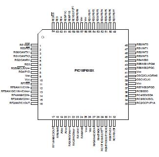
Block diagrams of the PIC18F6680 are provided in Figure 1-1 and Figure 1-2,respectively. The pinouts for these device families arelisted in Table 1-2.

 PIC18F6680 Data Sheet


