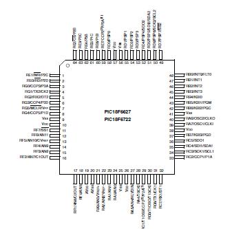
Features: • C compiler optimized architecture:
- Optional extended instruction set designed tooptimize re-entrant code
• 100,000 erase/write cycle Enhanced Flash programmemory typical
• 1,000,000 erase/write cycle Data EEPROM memory ypical
• Flash/Data EEPROM Retention: 100 years typical
• Self-programmable under software control
• Priority levels for interrupts
• 8 X 8 Single Cycle Hardware Multiplier
• Extended Watchdog Timer (WDT):
- Programmable period from 4 ms to 131s
• Single-supply In-Circuit Serial Programming™(ICSP™) via two pins
• In-Circuit Debug (ICD) via two pins
• Wide operating voltage range: 2.0V to 5.5V
Pinout Specifications
| Program Memory Type |
Flash |
| Program Memory (KB) |
96 |
| CPU Speed (MIPS) |
10 |
| RAM Bytes |
3,936 |
| Data EEPROM (bytes) |
1024 |
| Digital Communication Peripherals |
2-A/E/USART, 2-MSSP(SPI/I2C) |
| Capture/Compare/PWM Peripherals |
2 CCP, 3 ECCP |
| Timers |
2 x 8-bit, 3 x 16-bit |
| ADC |
12 ch, 10-bit |
| Comparators |
2 |
| Temperature Range (C) |
-40 to 125 |
| Operating Voltage Range (V) |
2 to 5.5 |
| Pin Count |
64 |
Ambient temperature under bias.......................................................................................................-40°C to +125°C
Storage temperature ....................................................................................................................... -65°C to +150°C
Voltage on any pin with respect to VSS (except VDD and MCLR) ................................................... -0.3V to (VDD + 0.3V)
Voltage on VDD with respect to VSS ........................................................................................................ -0.3V to +7.5V
Voltage onMCLR with respect to VSS (Note 2) ........................................................................................ 0V to +13.25V
Total power dissipation (Note 1) .............................................................................................................................1.0W
Maximum current out of VSS pin ...........................................................................................................................300 mA
Maximum current into VDD pin .............................................................................................................................250 mA
Input clamp current, IIK (VI < 0 or VI > VDD)...................................................................................................... ±20 mA
Output clamp current, IOK (VO < 0 or VO > VDD) ................................................................................................ ±20 mA
Maximum output current sunk by any I/O pin.........................................................................................................25 mA
Maximum output current sourced by any I/O pin ...................................................................................................25 mA
Maximum current sunk by all ports ......................................................................................................................200 mA
Maximum current sourced by all ports ..................................................................................................................200 mA
Note 1: Power dissipation is calculated as follows:Pdis = VDD x {IDD IOH} + {(VDD VOH) x IOH} + (VOL x IOL)
2: Voltage spikes below VSS at the MCLR/VPP/RG5 pin, inducing currents greater than 80 mA, may causelatch-up. Thus, a series resistor of 50-100 should be used when applying a "low" level to the MCLR/VPP/RG5 pin, rather than pulling this pin directly to VSS.
† NOTICE: Stresses above those listed under "Absolute Maximum Ratings" may cause permanent damage to thedevice. This is a stress rating only and functional operation of the device at those or any other conditions above thoseindicated in the operation listings of this specification is not implied. Exposure to maximum rating conditions forextended periods may affect device reliability.
DescriptionIdeal for large, low power (nanoWatt) and connectivity applications that benefit from the availability of four serial ports: double synchronous serial ports (I2C? and SPI?) and double asynchronous (LIN capable) serial ports. Large amounts of RAM memory PIC18F6627 for buffering and FLASH program memory make PIC18F6627 ideal for instrumentation panels, TCP/IP enabled embedded applications as well as metering and industrial control and monitoring applications.While operating up to 40 MHz, it is also backward software and hardware compatible with the PIC18F6720.
This document contains device specific information for he following devices:
• PIC18F6627 • PIC18LF6627
• PIC18F6722 • PIC18LF6722
• PIC18F8627 • PIC18LF8627
• PIC18F8722 • PIC18LF8722
This PIC18F6627 offers the advantages of all PIC18 microcontrollers namely, high computational performanceat an economical price with the addition of highendurace,Enhanced Flash program memory. On topof these features, the PIC18F6627 family introduces design enhancements that makethese microcontrollers a logical choice for many highperformance,power sensitive applications.

 PIC18F6627 Data Sheet


