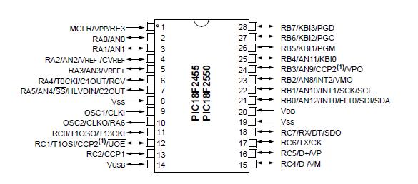
Features: • USB V2.0 Compliant
• Low Speed (1.5 Mb/s) and Full Speed (12 Mb/s)
• Supports Control, Interrupt, Isochronous and Bulk Transfers
• Supports up to 32 endpoints (16 bidirectional)
• 1-Kbyte dual access RAM for USB
• On-chip USB transceiver with on-chip voltage regulator
• Interface for off-chip USB transceiver
• Streaming Parallel Port (SPP) for USB streaming transfers (40/44-pin devices only)
Pinout Specifications
| Program Memory Type |
Flash |
| Program Memory (KB) |
24 |
| CPU Speed (MIPS) |
12 |
| RAM Bytes |
2,048 |
| Data EEPROM (bytes) |
256 |
| Digital Communication Peripherals |
1-A/E/USART, 1-MSSP(SPI/I2C) |
| Capture/Compare/PWM Peripherals |
1 CCP, 1 ECCP |
| Timers |
1 x 8-bit, 3 x 16-bit |
| ADC |
13 ch, 10-bit |
| Comparators |
2 |
| USB (ch, speed, compliance) |
1, Full Speed, USB 2.0 |
| Temperature Range (C) |
-40 to 85 |
| Operating Voltage Range (V) |
2 to 5.5 |
| Pin Count |
40 |
Absolute Maximum Ratings(†)
Ambient temperature under bias.............................................................. .-40°C to +85°C
Storage temperature .............................................................................. -65°C to +150°C
Voltage on any pin with respect to VSS (except VDD,MCLR and RA4)..-0.3V to (VDD + 0.3V)
Voltage on VDD with respect to VSS .............................................................. -0.3V to +7.5V
Voltage onMCLR with respect to VSS (Note 2) ............................................... 0V to +13.25V
Total power dissipation (Note 1) ....................................................................................1.0W
Maximum current out of VSS pin .................................................................................300 mA
Maximum current into VDD pin .....................................................................................250 mA
Input clamp current, IIK (VI < 0 or VI > VDD)............................................................. ±20 mA
Output clamp current, IOK (VO < 0 or VO > VDD) ....................................................... ±20 mA
Maximum output current sunk by any I/O pin................................................................25 mA
Maximum output current sourced by any I/O pin ..........................................................25 mA
Maximum current sunk by all ports ..............................................................................200 mA
Maximum current sourced by all ports ..........................................................................200 mA
Note 1: Power dissipation is calculated as follows:
Pdis = VDD x {IDD IOH} + {(VDD VOH) x IOH} + (VOL x IOL)
2: Voltage spikes below VSS at the MCLR/VPP/RE3 pin, inducing currents greater than 80 mA, may cause latch-up. Thus, a series resistor of 50-100 should be used when applying a "low" level to the MCLR/VPP/ RE3 pin, rather than pulling this pin directly to VSS.
† NOTICE: Stresses above those listed under "Absolute Maximum Ratings" may cause permanent damage to the
device. This is a stress rating only and functional operation of the device at those or any other conditions above those
indicated in the operation listings of this specification is not implied. Exposure to maximum rating conditions for extended periods may affect device reliability.
DescriptionIdeal for low power (nanoWatt) and connectivity applications that benefit from the availability of three serial ports: FS-USB(12Mbit/s), I2C? and SPI? (up to 10 Mbit/s) and an asynchronous (LIN capable) serial port (EUSART). Large amounts of RAM memory PIC18F4455 for buffering and Enhanced FLASH program memory make it ideal for embedded control and monitoring applications that require periodic connection with a (legacy free) Personal Computer via USB for data upload/download and/or firmware updates.While operating up to 48 MHz, the PIC18F4455 is also mostly software and hardware compatible with the PIC16C765 Low-Speed USB OTP devices.
USB Application Design Center

 PIC18F4455 Data Sheet


