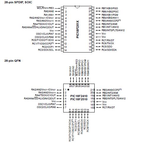
Features: • C compiler optimized architecture:- Optional extended instruction set designed to optimize re-entrant code• 100,000 erase/write cycle Flash program memory typical• Three programmable external interrupts• Four input-change interrupts• Priority levels for in...
PIC18F2X1X: Features: • C compiler optimized architecture:- Optional extended instruction set designed to optimize re-entrant code• 100,000 erase/write cycle Flash program memory typical• Thre...
SeekIC Buyer Protection PLUS - newly updated for 2013!
268 Transactions
All payment methods are secure and covered by SeekIC Buyer Protection PLUS.
SpecificationsDescriptionThe PIC1018SCL is one member of the PIC1018 family which is designed as o...
• C compiler optimized architecture:
- Optional extended instruction set designed to optimize re-entrant code
• 100,000 erase/write cycle Flash program memory typical
• Three programmable external interrupts
• Four input-change interrupts
• Priority levels for interrupts
• 8 x 8 Single-Cycle Hardware Multiplier
• Extended Watchdog Timer (WDT):
- Programmable period from 4 ms to 131s
• Single-supply 5V In-Circuit Serial Programming™ (ICSP™) via two pins
• In-Circuit Debug (ICD) via two pins
• Wide operating voltage range: 2.0V to 5.5V
• Programmable Brown-out Reset (BOR) with software enable option
Absolute Maximum Ratings(†)
Ambient temperature under bias.......................................................-40°C to +125°C
Storage temperature ....................................................................... -65°C to +150°C
Voltage on any pin with respect to VSS (except VDD and MCLR)..-0.3V to (VDD + 0.3V)
Voltage on VDD with respect to VSS ....................................................... -0.3V to +7.5V
Voltage on MCLR with respect to VSS (Note 2) ....................................... 0V to +13.25V
Total power dissipation (Note 1) ............................................................................1.0W
Maximum current out of VSS pin ..........................................................................300 mA
Maximum current into VDD pin .............................................................................250 mA
Input clamp current, IIK (VI < 0 or VI > VDD)..................................................... ±20 mA
Output clamp current, IOK (VO < 0 or VO > VDD) .............................................. ±20 mA
Maximum output current sunk by any I/O pin.........................................................25 mA
Maximum output current sourced by any I/O pin ....................................................25 mA
Maximum current sunk by all ports .......................................................................200 mA
Maximum current sourced by all ports ...................................................................200 mA
Note 1: Power dissipation is calculated as follows:
Pdis = VDD x {IDD IOH} + {(VDD VOH) x IOH} + (VOL x IOL)
2: Voltage spikes below VSS at the MCLR/VPP/RE3 pin, inducing currents greater than 80 mA, may cause latch-up. Thus, a series resistor of 50-100 should be used when applying a "low" level to the MCLR/VPP/ RE3 pin, rather than pulling this pin directly to VSS.
† NOTICE: Stresses above those listed under "Absolute Maximum Ratings" may cause permanent damage to the
device. This is a stress rating only and functional operation of the device at those or any other conditions above those
indicated in the operation listings of this specification is not implied. Exposure to maximum rating conditions for
extended periods may affect device reliability.