PIC18CXX2

Features: • High current sink/source 25 mA/25 mA• Three external interrupt pins• Timer0 module: 8-bit/16-bit timer/counter with 8-bit programmable prescaler• Timer1 module: 16-bit timer/counter• Timer2 module: 8-bit timer/counter with 8-bit period register (time-base ...

product image

PIC18CXX2 Picture
SeekIC No. : 004462097 Detail

PIC18CXX2: Features: • High current sink/source 25 mA/25 mA• Three external interrupt pins• Timer0 module: 8-bit/16-bit timer/counter with 8-bit programmable prescaler• Timer1 module: 1...

floor Price/Ceiling Price

Part Number:
PIC18CXX2
Supply Ability:
5000

Price Break

  • Qty
  • 1~5000
  • Unit Price
  • Negotiable
  • Processing time
  • 15 Days
Total Cost: $ 0.00

SeekIC Buyer Protection PLUS - newly updated for 2013!

  • Escrow Protection.
  • Guaranteed refunds.
  • Secure payments.
  • Learn more >>

Month Sales

268 Transactions

Rating

evaluate  (4.8 stars)

Upload time: 2025/1/10

Payment Methods

All payment methods are secure and covered by SeekIC Buyer Protection PLUS.

Notice: When you place an order, your payment is made to SeekIC and not to your seller. SeekIC only pays the seller after confirming you have received your order. We will also never share your payment details with your seller.
Product Details

Description


Features:

• High current sink/source 25 mA/25 mA
• Three external interrupt pins
• Timer0 module: 8-bit/16-bit timer/counter with 8-bit programmable prescaler
• Timer1 module: 16-bit timer/counter
• Timer2 module: 8-bit timer/counter with 8-bit period register (time-base for PWM)
• Timer3 module: 16-bit timer/counter
• Secondary oscillator clock option - Timer1/Timer3
• Two Capture/Compare/PWM (CCP) modules. CCP pins that can be configured as:
- Capture input: capture is 16-bit,max. resolution 6.25 ns (TCY/16)
- Compare is 16-bit, max. resolution 100 ns (TCY)
- PWM output: PWM resolution is 1- to 10-bit.
Max. PWM freq. @:8-bit resolution = 156 kHz 10-bit resolution= 39 kHz
• 10-bit Analog-to-Digital Converter module (A/D) with:
- Fast sampling rate
- Conversion available during sleep
- DNL = ±1 LSb, INL = ±1 LSb
• Programmable Low-Voltage Detection (LVD) module
- Supports interrupt on low voltage detection
• Programmable Brown-out Reset (BOR)


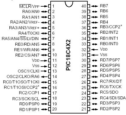
Pinout

  Connection Diagram


Specifications

Ambient temperature under bias.............................................................................................................-55°C to +125°C
Storage temperature .............................................................................................................................. -65°C to +150°C
Voltage on any pin with respect to VSS (except VDD, MCLR , and RA4).......................................... -0.3V to (VDD + 0.3V)
Voltage on VDD with respect to VSS ......................................................................................................... -0.3V to +7.5V
Voltage on MCLR  with respect to VSS (Note 2).......................................................................................... 0V to +13.25V
Voltage on RA4 with respect to Vss ............................................................................................................... 0V to +8.5V
Total power dissipation (Note 1)...............................................................................................................................1.0W
Maximum current out of VSS pin ...........................................................................................................................300 mA
Maximum current into VDD pin ..............................................................................................................................250 mA
Input clamp current, IIK (VI < 0 or VI > VDD)...................................................................................................................... ±20 mA
Output clamp current, IOK (VO < 0 or VO > VDD) .............................................................................................................. ±20 mA
Maximum output current sunk by any I/O pin..........................................................................................................25 mA
Maximum output current sourced by any I/O pin ....................................................................................................25 mA
Maximum current sunk by PORTA, PORTB, and PORTE (Note 3) (combined)....................................................200 mA
Maximum current sourced by PORTA, PORTB, and PORTE (Note 3) (combined) ..............................................200 mA
Maximum current sunk by PORTC and PORTD (Note 3) (combined) ..................................................................200 mA
Maximum current sourced by PORTC and PORTD (Note 3) (combined) .............................................................200 mA


Customers Who Bought This Item Also Bought

Margin,quality,low-cost products with low minimum orders. Secure your online payments with SeekIC Buyer Protection.
Programmers, Development Systems
Potentiometers, Variable Resistors
Fans, Thermal Management
Resistors
Industrial Controls, Meters
RF and RFID
View more