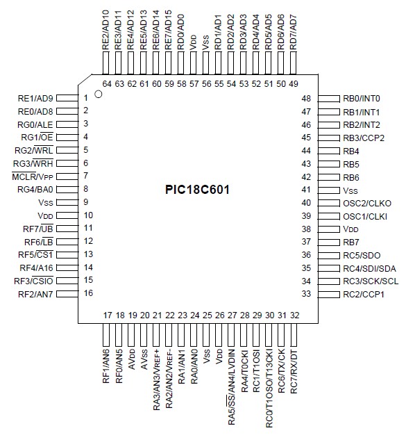
Features: • 10-bit Analog-to-Digital Converter module (A/D) ith:- Fast sampling rate- Conversion available during SLEEP- DNL = ±1 LSb, INL = ±1 LSb- Up to 12 channels available• Programmable Low Voltage Detection (LVD) odule- Supports interrupt on Low Voltage DetectionSpecificationsAmb...
PIC18C601_1166381: Features: • 10-bit Analog-to-Digital Converter module (A/D) ith:- Fast sampling rate- Conversion available during SLEEP- DNL = ±1 LSb, INL = ±1 LSb- Up to 12 channels available• Programm...
SeekIC Buyer Protection PLUS - newly updated for 2013!
268 Transactions
All payment methods are secure and covered by SeekIC Buyer Protection PLUS.
SpecificationsDescriptionThe PIC1018SCL is one member of the PIC1018 family which is designed as o...
Ambient temperature under bias.........................................................................................................-55°C to +125°C
Storage temperature ......................................................................................................................... -65°C to +150°C
Voltage on any pin with respect to VSS (except VDD, MCLR, and RA4) ......................................... -0.3V to (VDD + 0.3V)
Voltage on VDD with respect to VSS ......................................................................................................... -0.3V to +7.5V
Voltage on MCLR with respect to VSS (Note 2) ......................................................................................... 0V to +13.25V
Voltage on RA4 with respect to VSS............................................................................................................... 0V to +8.5V
Total power dissipation (Note1) ...............................................................................................................................1.0W
Maximum current out of VSS pin ...........................................................................................................................300 mA
Maximum current into VDD pin ..............................................................................................................................250 mA
Input clamp current, IIK (VI < 0 or VI >VDD)........................................................................................................ ±20 mA
Output clamp current, IOK (VO < 0 or VO >VDD) ................................................................................................. ±20 mA
Maximum output current sunk by any I/O pin..........................................................................................................25 mA
Maximum output current sourced by any I/O pin ....................................................................................................25 mA
Maximum current sunk by all ports (combined) ....................................................................................................200 mA
Maximum current sourced by all ports (combined) ...............................................................................................200 mA
Note 1: Power dissipation is calculated as follows: dis = VDD x {IDD - IOH} + {(VDD-VOH) x IOH} + (VOl x IOL)
2: Voltage spikes below VSS at the MCLR/VPP pin, inducing currents greater than 80 mA, may cause latch-up. hus, a series resistor of 50-100 should be used when applying a "low" level to the MCLR/VPP pin, rather han pulling this pin directly to VSS