PIC17C75X

Features: Microcontroller Core Features:• Only 58 single word instructions to learn• All single cycle instructions (121 ns) except for program branches and table reads/writes which are two-cycle• Operating speed: - DC - 33 MHz clock input - DC - 121 ns instruction cycle• Ha...

product image

PIC17C75X Picture
SeekIC No. : 004462061 Detail

PIC17C75X: Features: Microcontroller Core Features:• Only 58 single word instructions to learn• All single cycle instructions (121 ns) except for program branches and table reads/writes which are t...

floor Price/Ceiling Price

Part Number:
PIC17C75X
Supply Ability:
5000

Price Break

  • Qty
  • 1~5000
  • Unit Price
  • Negotiable
  • Processing time
  • 15 Days
Total Cost: $ 0.00

SeekIC Buyer Protection PLUS - newly updated for 2013!

  • Escrow Protection.
  • Guaranteed refunds.
  • Secure payments.
  • Learn more >>

Month Sales

268 Transactions

Rating

evaluate  (4.8 stars)

Upload time: 2024/11/25

Payment Methods

All payment methods are secure and covered by SeekIC Buyer Protection PLUS.

Notice: When you place an order, your payment is made to SeekIC and not to your seller. SeekIC only pays the seller after confirming you have received your order. We will also never share your payment details with your seller.
Product Details

Description


Features:

Microcontroller Core Features:
• Only 58 single word instructions to learn
• All single cycle instructions (121 ns) except for program branches and table reads/writes which are two-cycle
• Operating speed:
   - DC - 33 MHz clock input
   - DC - 121 ns instruction cycle
• Hardware Multiplier
• Interrupt capability
• 16 level deep hardware stack
• Direct, indirect, and relative addressing modes
• Internal/external program memory execution
• Capable of addressing 64K x 16 program memory space
Peripheral Features:
• 50 I/O pins with individual direction control
• High current sink/source for direct LED drive
   - RA2 and RA3 are open drain, high voltage(12V), high current (60 mA), I/O pins
• Four capture input pins
   - Captures are 16-bit, max resolution 121 ns
• Three PWM outputs
   - PWM resolution is 1- to 10-bits
• TMR0: 16-bit timer/counter with 8-bit programmable prescaler
• TMR1: 8-bit timer/counter
• TMR2: 8-bit timer/counter
• TMR3: 16-bit timer/counter
• Two Universal Synchronous Asynchronous Receiver Transmitters (USART/SCI)
- Independant baud rate generators
• 10-bit, 12 channel analog-to-digital converter
• Synchronous Serial Port (SSP) with SPI™ and I2C™ modes (including I2C master mode)
Special Microcontroller Features:
• Power-on Reset (POR), Power-up Timer (PWRT) and Oscillator Start-up Timer (OST)
• Watchdog Timer (WDT) with its own on-chip RC oscillator for reliable operation
• Brown-out Reset
• Code-protection
• Power saving SLEEP mode
• Selectable oscillator options


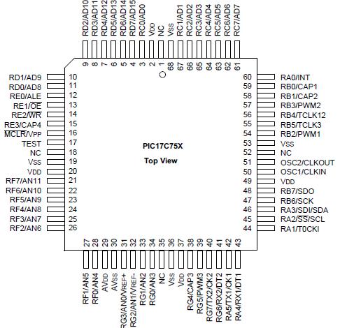
Pinout

  Connection Diagram


Specifications

Ambient temperature under bias............................................. -55 to +125°C
Storage temperature ......................................................... -65°C to +150°C
Voltage on VDD with respect to VSS ................................................ 0 to +7.5V
Voltage on MCLR with respect to VSS (Note 2)........................... -0.3V to +14V
Voltage on RA2 and RA3 with respect to VSS...............................-0.3V to +14V
Voltage on all other pins with respect to VSS ................... -0.3V to VDD + 0.3V
Total power dissipation (Note 1)................................................................1.0W
Maximum current out of VSS pin(s) - total (@ 70°C) .............................500 mA
Maximum current into VDD pin(s) - total (@ 70°C) ................................500 mA
Input clamp current, IIK (VI < 0 or VI > VDD) ........................................±20 mA
Output clamp current, IOK (VO < 0 or VO > VDD) ..................................±20 mA
Maximum output current sunk by any I/O pin (except RA2 and RA3)........35 mA
Maximum output current sunk by RA2 or RA3 pins ...................................60 mA
Maximum output current sourced by any I/O pin ......................................20 mA
Maximum current sunk by PORTA and PORTB (combined) .......................150 mA
Maximum current sourced by PORTA and PORTB (combined)...................100 mA
Maximum current sunk by PORTC, PORTD and PORTE (combined)............150 mA
Maximum current sourced by PORTC, PORTD and PORTE (combined).......100 mA
Maximum current sunk by PORTF and PORTG (combined) ........................150 mA
Maximum current sourced by PORTF and PORTG (combined) ...................100 mA

Note 1: Power dissipation is calculated as follows: Pdis = VDD x {IDD - IOH} + {(VDD-VOH) x IOH} + (VOL x IOL) Note 2: Voltage spikes below VSS at the MCLR pin, inducing currents greater than 80 mA, may cause latch-up. Thus,a series resistor of 50-100W should be used when applying a "low" level to the MCLR pin rather than pulling this pin directly to VSS.

† NOTICE: Stresses above those listed under "Absolute Maximum Ratings" may cause permanent damage to the device. This is a stress rating only and functional operation of the device at those or any other conditions above those indicated in the operation listings of this specification is not implied. Exposure to maximum rating conditions for extended periods may affect device reliability.


Customers Who Bought This Item Also Bought

Margin,quality,low-cost products with low minimum orders. Secure your online payments with SeekIC Buyer Protection.
Transformers
Isolators
Undefined Category
RF and RFID
Potentiometers, Variable Resistors
View more