Features: Low-Power Features:
• Power-Managed modes:
- Primary Run: RC oscillator, 76 A, 1 MHz, 2V
- RC_RUN: 7 A, 31.25 kHz, 2V
- SEC_RUN: 9 A, 32 kHz, 2V
- Sleep: 0.1 A, 2V
• Timer1 Oscillator: 1.8 A, 32 kHz, 2V
• Watchdog Timer: 2.2 A, 2V
• Two-Speed Oscillator Start-up
Peripheral Features:
• Capture, Compare, PWM (CCP) module:
- Capture is 16-bit, max. resolution is 12.5 ns
- Compare is 16-bit, max. resolution is 200 ns
- PWM max. resolution is 10-bit
• 10-bit, 7-channel Analog-to-Digital Converter
• Synchronous Serial Port (SSP) with SPI™ (Master/Slave) and I2C™ (Slave)
• Addressable Universal Synchronous Asynchronous Receiver Transmitter (AUSART/SCI) with 9-bit address detection:
- RS-232 operation using internal oscillator (no external crystal required)
• Dual Analog Comparator module:
- Programmable on-chip voltage reference
- Programmable input multiplexing from device inputs and internal voltage reference
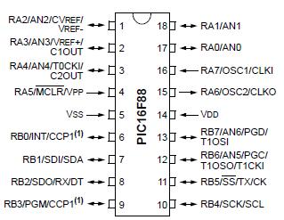
- Comparator outputs are externally accessible Pin Diagram
Special Microcontroller Features:
• 100,000 erase/write cycles Enhanced Flash program memory typical
• 1,000,000 typical erase/write cycles EEPROM data memory typical
• EEPROM Data Retention: > 40 years
• In-Circuit Serial Programming™ (ICSP™) via two pins
• Processor read/write access to program memory
• Low-Voltage Programming
• In-Circuit Debugging via two pins
• Extended Watchdog Timer (WDT):
- Programmable period from 1 ms to 268s
• Wide operating voltage range: 2.0V to 5.5V
Pinout Specifications
Absolute Maximum Ratings †
Ambient temperature under bias.....................................................-40°C to +125°C
Storage temperature ..................................................................... -65°C to +150°C
Voltage on any pin with respect to VSS (except VDD and MCLR)..-0.3V to (VDD + 0.3V)
Voltage on VDD with respect to VSS ........................................................ -0.3 to +7.5V
Voltage onMCLR with respect to VSS(Note 2)...........................................-0.3 to +14V
Total power dissipation (Note 1) ..............................................................................1W
Maximum current out of VSS pin ..........................................................................200 mA
Maximum current into VDD pin .............................................................................200 mA
Input clamp current, IIK (VI < 0 or VI > VDD)....................................................... ±20 mA
Output clamp current, IOK (VO < 0 or VO > VDD)...................................................±20 mA
Maximum output current sunk by any I/O pin...........................................................25 mA
Maximum output current sourced by any I/O pin......................................................25 mA
Maximum current sunk by PORTA.............................................................................100 mA
Maximum current sourced by PORTA........................................................................100 mA
Maximum current sunk by PORTB.............................................................................100 mA
Maximum current sourced by PORTB .......................................................................100 mA
Note 1: Power dissipation is calculated as follows: Pdis = VDD x {IDD IOH} + {(VDD VOH) x IOH} + (VOL x IOL)
2: Voltage spikes at theMCLR pin may cause latch-up. A series resistor of greater than 1 k should be used
to pullMCLR to VDD, rather than tying the pin directly to VDD.
† NOTICE: Stresses above those listed under "Absolute Maximum Ratings" may cause permanent damage to the
device. This is a stress rating only and functional operation of the device at those or any other conditions above those
indicated in the operation listings of this specification is not implied. Exposure to maximum rating conditions for
extended periods may affect device reliability.
| Program Memory Type |
Flash |
| Program Memory (KB) |
7 |
| CPU Speed (MIPS) |
5 |
| RAM Bytes |
368 |
| Data EEPROM (bytes) |
256 |
| Digital Communication Peripherals |
1-A/E/USART, 1-SSP(SPI/I2C) |
| Capture/Compare/PWM Peripherals |
1 CCP |
| Timers |
2 x 8-bit, 1 x 16-bit |
| ADC |
7 ch, 10-bit |
| Comparators |
2 |
| Temperature Range (C) |
-40 to 125 |
| Operating Voltage Range (V) |
2 to 5.5 |
| Pin Count |
18 |
DescriptionThis powerful (200 nanosecond instruction execution) yet easyto-program (only 35 single word instructions) CMOS Flash-based 8-bit microcontroller packs Microchip's powerful PIC? architecture into an 18-pin package and is upwards compatible with the PIC16C7x, PIC16C62xA, PIC16C5X and PIC12CXXX devices. The PIC16F88 features 8 MHz internal oscillator, 256 bytes of EEPROM data memory, a capture/compare/PWM, an Addressable USART, a synchronous serial port that can be configured as either 3-wire Serial Peripheral Interface (SPI?) or the 2-wire Inter-Integrated Circuit (I2C?) bus, 7 channels of 10-bit Analog-to-Digital (A/D) converter and 2 Comparators that make PIC16F88 ideal for advantage analog / integrated level applications in automotive, industrial, appliances and consumer applications.

 PIC16F88 Data Sheet


