PIC16F7X

Features: • Timer0: 8-bit timer/counter with 8-bit prescaler• Timer1: 16-bit timer/counter with prescaler, can be incremented during SLEEP via external crystal/clock• Timer2: 8-bit timer/counter with 8-bit period register, prescaler and postscaler• Two Capture, Compare, PWM...

product image

PIC16F7X Picture
SeekIC No. : 004461933 Detail

PIC16F7X: Features: • Timer0: 8-bit timer/counter with 8-bit prescaler• Timer1: 16-bit timer/counter with prescaler, can be incremented during SLEEP via external crystal/clock• Timer2: 8-bit...

floor Price/Ceiling Price

Part Number:
PIC16F7X
Supply Ability:
5000

Price Break

  • Qty
  • 1~5000
  • Unit Price
  • Negotiable
  • Processing time
  • 15 Days
Total Cost: $ 0.00

SeekIC Buyer Protection PLUS - newly updated for 2013!

  • Escrow Protection.
  • Guaranteed refunds.
  • Secure payments.
  • Learn more >>

Month Sales

268 Transactions

Rating

evaluate  (4.8 stars)

Upload time: 2024/11/25

Payment Methods

All payment methods are secure and covered by SeekIC Buyer Protection PLUS.

Notice: When you place an order, your payment is made to SeekIC and not to your seller. SeekIC only pays the seller after confirming you have received your order. We will also never share your payment details with your seller.
Product Details

Description


Features:

• Timer0: 8-bit timer/counter with 8-bit prescaler
• Timer1: 16-bit timer/counter with prescaler, can be incremented during SLEEP via external crystal/clock
• Timer2: 8-bit timer/counter with 8-bit period register, prescaler and postscaler
• Two Capture, Compare, PWM modules
- Capture is 16-bit, max. resolution is 12.5 ns
- Compare is 16-bit, max. resolution is 200 ns
- PWM max. resolution is 10-bit
• 8-bit multi-channel Analog-to-Digital converter
• Synchronous Serial Port (SSP) with SPI™ (Master mode) and I2C (Slave)
• Universal Synchronous Asynchronous Receiver Transmitter (USART/SCI)
• Parallel Slave Port (PSP) 8-bits wide, with external RDWR and CS controls (40/44-pin only)
• Brown-out detection circuitry for Brown-out Reset (BOR)


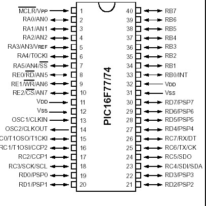
Pinout

  Connection Diagram


Specifications

Ambient temperature under bias.......................................................................................... .-55 to +125°C
Storage temperature ....................................................................................................... -65°C to +150°C
Voltage on any pin with respect to VSS (except VDD, MCLR. and RA4) ....................... -0.3V to (VDD + 0.3V)
Voltage on VDD with respect to VSS ........................................................................................ -0.3 to +6.5V
Voltage on MCLR with respect to VSS (Note 2)............................................................................0 to +13.5V
Voltage on RA4 with respect to Vss ...............................................................................................0 to +12V
Total power dissipation (Note 1)............................................................................................................1.0W
Maximum current out of VSS pin ........................................................................................................300 mA
Maximum current into VDD pin ...........................................................................................................250 mA
Input clamp current, IIK (VI < 0 or VI > VDD).................................................................................. ± 20 mA
Output clamp current, IOK (VO < 0 or VO > VDD) ........................................................................... ± 20 mA
Maximum output current sunk by any I/O pin.......................................................................................25 mA
Maximum output current sourced by any I/O pin .................................................................................25 mA
Maximum current sunk by PORTA, PORTB, and PORTE (combined) (Note 3) .......................................200 mA
Maximum current sourced by PORTA, PORTB, and PORTE (combined) (Note 3) ..................................200 mA
Maximum current sunk by PORTC and PORTD (combined) (Note 3) ....................................................200 mA
Maximum current sourced by PORTC and PORTD (combined) (Note 3)................................................200 mA
Note 1: Power dissipation is calculated as follows: Pdis = VDD x {IDD - IOH} + {(VDD - VOH) x IOH} + (VOl x IOL)
2: Voltage spikes below VSS at the MCLR pin, inducing currents greater than 80 mA, may cause latch-up. Thus, a series resistor of 50-100Ω should be used when applying a "low" level to the MCLR pin, rather than pulling this pin directly to VSS.
3: PORTD and PORTE are not implemented on the PIC16F73/76 devices.


Customers Who Bought This Item Also Bought

Margin,quality,low-cost products with low minimum orders. Secure your online payments with SeekIC Buyer Protection.
Tapes, Adhesives
803
Potentiometers, Variable Resistors
Discrete Semiconductor Products
LED Products
Semiconductor Modules
View more