PIC16CR7X

Features: • Power-on Reset (POR)• Power-up Timer (PWRT) and Oscillator Start-up Timer (OST)• Watchdog Timer (WDT) with its own on-chip RC oscillator for reliable operation• Power-Saving Sleep mode• Selectable oscillator optionsPinoutSpecificationsAmbient temperature u...

product image

PIC16CR7X Picture
SeekIC No. : 004461811 Detail

PIC16CR7X: Features: • Power-on Reset (POR)• Power-up Timer (PWRT) and Oscillator Start-up Timer (OST)• Watchdog Timer (WDT) with its own on-chip RC oscillator for reliable operation• P...

floor Price/Ceiling Price

Part Number:
PIC16CR7X
Supply Ability:
5000

Price Break

  • Qty
  • 1~5000
  • Unit Price
  • Negotiable
  • Processing time
  • 15 Days
Total Cost: $ 0.00

SeekIC Buyer Protection PLUS - newly updated for 2013!

  • Escrow Protection.
  • Guaranteed refunds.
  • Secure payments.
  • Learn more >>

Month Sales

268 Transactions

Rating

evaluate  (4.8 stars)

Upload time: 2024/11/25

Payment Methods

All payment methods are secure and covered by SeekIC Buyer Protection PLUS.

Notice: When you place an order, your payment is made to SeekIC and not to your seller. SeekIC only pays the seller after confirming you have received your order. We will also never share your payment details with your seller.
Product Details

Description


Features:

• Power-on Reset (POR)
• Power-up Timer (PWRT) and Oscillator Start-up Timer (OST)
• Watchdog Timer (WDT) with its own on-chip RC oscillator for reliable operation
• Power-Saving Sleep mode
• Selectable oscillator options


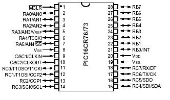
Pinout

  Connection Diagram


Specifications

Ambient temperature under bias............................................... -55 to +125°C
Storage temperature ............................................................ -65°C to +150°C
Voltage on any pin with respect to VSS .......................... -0.3V to (VDD + 0.3V)
Voltage on VDD with respect to VSS ............................................ -0.3 to +6.5V
Voltage on MCLR with respect to VSS................................................0 to +5.5V
Voltage on RA4 with respect to Vss ..................................................0 to +5.5V
Total power dissipation (Note 1) ..............................................................1.0W
Maximum current out of VSS pin ............................................................300 mA
Maximum current into VDD pin ...............................................................250 mA
Input clamp current, IIK (VI < 0 or VI > VDD)....................................... ± 20 mA
Output clamp current, IOK (VO < 0 or VO > VDD) ................................. ± 20 mA
Maximum output current sunk by any I/O pin..........................................25 mA
Maximum output current sourced by any I/O pin ....................................25 mA
Maximum current sunk by PORTA, PORTB, and PORTE (combined)  .......200 mA
Maximum current sourced by PORTA, PORTB, and PORTE (combined) ...200 mA
Maximum current sunk by PORTC and PORTD (combined)  ....................200 mA
Maximum current sourced by PORTC and PORTD (combined)  ...............200 mA


Customers Who Bought This Item Also Bought

Margin,quality,low-cost products with low minimum orders. Secure your online payments with SeekIC Buyer Protection.
Memory Cards, Modules
Semiconductor Modules
LED Products
RF and RFID
Static Control, ESD, Clean Room Products
View more