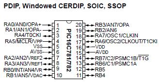
Features: • High performance RISC CPU
• Only 35 single word instructions to learn
• All single cycle instructions except for program branches which are two cycle
• Direct, indirect and relative addressing modes
- Operating speed: DC - 20 MHz clock input DC - 200 ns instruction cycle
• 8-level deep hardware stack
• Interrupt capability (up to 8 internal/external interrupt sources)
• 16 I/O pins:
- Individual direction control (13 pins)
- Input only (3 pins), low leakage (2 pins)
- Digital/Analog inputs (8 pins)
• Programmable PORTB interrupt-on-change (8 pins)
• Programmable PORTB weak pull-ups (8 pins)
• Power-on Reset (POR)
• Power-up Timer (PWRT) and Oscillator Start-up Timer (OST)
• Watchdog Timer (WDT) with a software enabled
option and its own on-chip RC oscillator for reliable operation
• Programmable Brown-out Reset (BOR)
• Programmable Low Voltage Detection (LVD)
• Internal/external MCLR
• Programmable code protection
• Power saving SLEEP mode
• Selectable oscillator options: HS, XT, LP, EC, RC, INTRC (4 MHz/37 kHz)
• In-Circuit Serial Programming™ (ISCP™)
• Program Memory Read (PMR) capability
• Four user programmable ID locations
• Wide operating voltage range:
- 2.5V to 5.5V for commercial and industrial temperature ranges
- Extended temperature range available
Microcontroller Core Features (Continued):
• Low power, high speed CMOS EPROM technology
• Fully static design
• Low power consumption:
- < 2 mA @ 5V, 4 MHz
- < 1 A typical standby current.
Peripheral Features:
• Timer0: 8-bit timer/counter with 8-bit prescaler
• Enhanced Timer1:
- 16-bit timer/counter with prescaler
- External Gate Input mode
- Option to use OSC1 and OSC2 in LP mode as Timer1 oscillator, if INTRC oscillator mode selected
• Analog-to-Digital Converter (ADC):
- 8-bit resolution
- Programmable 8-channel input
- Internal voltages available for selfdiagnostics
• Digital-to-Analog Converter (DAC):
- 8-bit resolution
- Reference from AVDD, VREF1, or VR module
- Output configurable to VDAC pin, Comparators, and ADC reference
• Operational Amplifier module (OPA):
- Firmware initiated input offset voltage Auto Calibration module
- Low leakage inputs
- Programmable Gain Bandwidth Product (GBWP)
Peripheral Features (Continued):
• Dual Analog Comparator module with:
- Individual enable and interrupt bits
- Programmable speed and output polarity
- Fully configurable inputs and outputs
- Reference from DAC, or VREF1/VREF2
- Low input offset voltage.
• VR voltage reference module:
- 3.072V +/- 0.7% @25°C, AVDD = 5V
- Configurable output to ADC reference, DAC reference, and VR pin
- 5 mA sink/source
• Programmable Switch Mode Controller module:
- PWM and PSM modes
- Programmable switching frequency
- Configurable for either single or dual feedback inputs
- Configurable single or dual outputs
- Slope compensation output available in single output modePinout Specifications
Absolute Maximum Ratings †
Ambient temperature under bias................................................................. -55°C to +125°C
Storage temperature .................................................................................. -65°C to +150°C
Voltage on any pin with respect to VSS (except VDD,MCLR and RA4)...-0.3V to (VDD + 0.3 V)
Voltage on VDD with respect to VSS ..................................................................-0.3 to +7.5 V
Maximum voltage between AVDD and VDD pins............................................................± 0.3 V
Maximum voltage between AVSS and VSS pins.............................................................± 0.3 V
Voltage onMCLR with respect to VSS.............................................................. -0.3 V to +8.5 V
Voltage on RA4 with respect to Vss ................................................................0.3 V to +10.5 V
Total power dissipation(1) (PDIP, SOIC).......................................................................... 1.0 W
Total power dissipation(1) (SSOP)................................................................................. 0.65 W
Maximum current out of VSS pin ................................................................................... 300 mA
Maximum current into VDD pin ...................................................................................... 250 mA
Input clamp current, IIK (VI < 0 or VI > VDD ................................................................ ± 20 mA
Output clamp current, IOK (VO < 0 or VO > VDD ........................................................... ± 20 mA
Maximum output current sunk by any I/O pin................................................................... 25 mA
Maximum output current sourced by any I/O pin ............................................................. 25 mA
Maximum current sunk by PORTA and PORTB (combined)................................................ 200 mA
Maximum current sourced by PORTA and PORTB (combined............................................. 200 mA
Note 1: Power dissipation is calculated as follows: PDIS = VDD x {IDD - IOH} + {(VDD - VOH) x IOH} + (VOL x IOL).
† NOTICE: Stresses above those listed under "Absolute Maximum Ratings" may cause permanent damage to the
device. This is a stress rating only and functional operation of the device at those or any other conditions above those
indicated in the operation listings of this specification is not implied. Exposure to maximum rating conditions for
extended periods may affect device reliability.
| Program Memory Type |
OTP |
| Program Memory (KB) |
1.75 |
| CPU Speed (MIPS) |
5 |
| RAM Bytes |
128 |
| Timers |
2 x 8-bit, 1 x 16-bit |
| ADC |
8 ch, 8-bit |
| Comparators |
2 |
| Temperature Range (C) |
-40 to 85 |
| Operating Voltage Range (V) |
2.5 to 5.5 |
| Pin Count |
20 |
DescriptionThis powerful (200 nanosecond instruction execution) yet easy-to-program (only 35 single word instructions) CMOS OTP-based 8-bit microcontroller packs Microchip's powerful PIC? architecture into an 20-pin package and is upwards compatible with the PIC16C5X and PIC12CXXX devices. The PIC16C781 features the highest level of analog peripheral features in any PICmicro? microcontroller to date. With 6 various fully integrated, mixed signal analog peripherals in a 20-pin package. Thus saving component cost and board space as well as critical design time by using firmware to control the changing interconnections and analog parameters. This makes PIC16C781 the most sophisticated Analog microcontroller device applications and ideal for automotive, industrial, appliances and consumer applications.

 PIC16C781 Data Sheet


