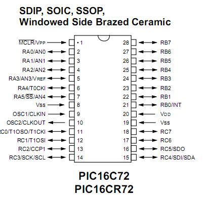
Features: * High-performance RISC CPU* Only 35 single word instructions to learn* All single cycle instructions except for program branches which are two cycle* Operating speed: DC - 20 MHz clock input DC - 200 ns instruction cycle* 2K x 14 words of Program Memory, 128 x 8 bytes of Data Memory (RA...
PIC16C72: Features: * High-performance RISC CPU* Only 35 single word instructions to learn* All single cycle instructions except for program branches which are two cycle* Operating speed: DC - 20 MHz clock in...
SeekIC Buyer Protection PLUS - newly updated for 2013!
268 Transactions
All payment methods are secure and covered by SeekIC Buyer Protection PLUS.
SpecificationsDescriptionThe PIC1018SCL is one member of the PIC1018 family which is designed as o...
Parameter |
PIC16C72 |
PIC16CR72 |
Ambient temperature under bias |
-55 to +125˚C |
-55 to +125˚C |
Storage temperature |
-65˚C to +150˚C |
-65˚C to +150˚C |
Voltage on any pin with respect to VSS (except VDD, MCLR, and RA4) |
-0.3V to (VDD + 0.3V) |
Voltage on VDD with respect to VSS |
-0.3 to +7.5V |
TBD |
Voltage on MCLRwith respect to VSS (Note 1) |
-0.3 to +14V |
TBD |
Voltage on RA4 with respect to Vss |
-0.3 to +14V |
TBD |
Total power dissipation (Note 2) |
1.0W |
1.0W |
Maximum current out of VSS pin |
300 mA |
300 mA |
Maximum current into VDD pin |
25 0mA |
250 mA |
Input clamp current, IIK (VI < 0 or VI > VDD) |
± 20 mA |
± 20 mA |
Output clamp current, IOK (VO < 0 or VO > VDD) |
± 20 mA |
± 20 mA |
Maximum output current sunk by any I/O pin |
25 mA |
25 mA |
Maximum output current sourced by any I/O pin |
25 mA |
25 mA |
Maximum current sunk by PORTA and PORTB (combined) |
200 mA |
200 mA |
Maximum current sourced by PORTA and PORTB (combined) |
200 mA |
200 mA |
Maximum current sunk by PORTC |
200 mA |
200 mA |
Maximum current sourced by PORTC |
200 mA |
200 mA |
1. Voltage spikes below VSS at the MCLR pin, inducing currents greater than 80 mA, may cause latch-up. Thus, a series resistor of 50-100Ω should be used when applying a "low" level to the MCLR pin rather than pulling this pin directly to VSS.
2. Power dissipation is calculated as follows: Pdis = VDD x {IDD - IOH} + {(VDD - VOH) x IOH} + (VOl x IOL).
Parameter Name | Value |
Program Memory Type | OTP |
Program Memory (KB) | 3.5 |
CPU Speed (MIPS) | 5 |
RAM Bytes | 128 |
Digital Communication Peripherals | 1-SSP(SPI/I2C) |
Capture/Compare/PWM Peripherals | 1 CCP |
Timers | 2 x 8-bit, 1 x 16-bit |
ADC | 5 ch, 8-bit |
Temperature Range (C) | -40 to 85 |
Operating Voltage Range (V) | 2.5 to 6 |
Pin Count | 28 |
Each PIC16CXXX family instruction is a 14-bit word divided into an OPCODE which specifies the instruction type and one or more operands which further specify the operation of the instruction. The PIC16CXXX family instruction set summary in Table 11-2 lists byteoriented, bit-oriented, and literal and control operations. Table 11-1 shows the opcode field descriptions.
For byte-oriented instructions, 'f' represents a file register designator and 'd' represents a destination designator. The file register designator specifies which file register is to be used by the instruction.
The destination designator specifies where the result of the operation is to be placed. If 'd' is zero, the result is placed in the W register. If 'd' is one, the result is placed in the file register specified in the instruction.
For bit-oriented instructions, 'b' represents a bit field designator which selects the number of the bit affected by the operation, while 'f' represents the number of the file in which the bit is located.
For literal and control operations, 'k' represents an eight or eleven bit constant or literal value.