PIC12F506

Features: Special Microcontroller Features:• 4 or 8 MHz selectable precision internal oscillator:- Factory calibrated to ±1%• In-Circuit Serial Programming™ (ICSP™)• In-Circuit Debugging (ICD) support• Power-on Reset (POR)• Device Reset Timer (DRT)- Short ...

product image

PIC12F506 Picture
SeekIC No. : 004461530 Detail

PIC12F506: Features: Special Microcontroller Features:• 4 or 8 MHz selectable precision internal oscillator:- Factory calibrated to ±1%• In-Circuit Serial Programming™ (ICSP™)• In...

floor Price/Ceiling Price

Part Number:
PIC12F506
Supply Ability:
5000

Price Break

  • Qty
  • 1~5000
  • Unit Price
  • Negotiable
  • Processing time
  • 15 Days
Total Cost: $ 0.00

SeekIC Buyer Protection PLUS - newly updated for 2013!

  • Escrow Protection.
  • Guaranteed refunds.
  • Secure payments.
  • Learn more >>

Month Sales

268 Transactions

Rating

evaluate  (4.8 stars)

Upload time: 2025/1/10

Payment Methods

All payment methods are secure and covered by SeekIC Buyer Protection PLUS.

Notice: When you place an order, your payment is made to SeekIC and not to your seller. SeekIC only pays the seller after confirming you have received your order. We will also never share your payment details with your seller.
Product Details

Description


Features:

Special Microcontroller Features:
• 4 or 8 MHz selectable precision internal oscillator:
- Factory calibrated to ±1%
• In-Circuit Serial Programming™ (ICSP™)
• In-Circuit Debugging (ICD) support
• Power-on Reset (POR)
• Device Reset Timer (DRT)
- Short DRT (1.125 ms, typical) for INTOSC, EXTRC and EC
- DRT (18 ms, typical) for HS, XT and LP
• Watchdog Timer (WDT) with dedicated on-chip RC oscillator for reliable operation
• Programmable code protection
• Multiplexed MCLR input pin
• Selectable internal weak pull-ups on I/O pins
• Power-saving Sleep mode
• Wake-up from Sleep on pin change
• Wake-up from Sleep on comparator change
• Selectable oscillator options:
- INTOSC: 4/8 MHz precision Internal oscillator
- EXTRC: External low-cost RC oscillator
- XT: Standard crystal/resonator
- HS: High-speed crystal/resonator (PIC16F506 only)
- LP: Power-saving, low-frequency crystal
- EC: High-speed external clock input (PIC16F506 only)
• Analog-to-Digital (A/D) Converter
- 8-bit resolution
- 4-input channels (1 channel is dedicated to conversion of the internal 0.6V absolute voltage reference)
• High current sink/source for direct LED drive
• 8-bit real-time clock/counter (TMR0) with 8-bit programmable prescaler

Low-Power Features/CMOS Technology:
• Operating Current:
- < 350 A @ 2V, 4 MHz
• Standby Current:
- 100 nA @ 2V, typical
• Low-power, high-speed Flash technology:
- 100,000 cycle Flash endurance
- > 40-year retention
• Fully static design
• Wide operating voltage range: 2.0V to 5.5V
• Wide temperature range:
- Industrial: -40°C to +85°C
- Extended: -40°C to +125°C

Peripheral Features (PIC12F510):
• 6 I/O pins:
- 5 I/O pins with individual direction control
- 1 input only pin
• 1 Analog Comparator with absolute reference

Peripheral Features (PIC16F506):
• 12 I/O pins:
- 11 I/O pins with individual direction control
- 1 input only pin
• 2 Analog Comparators with absolute reference and programmable reference


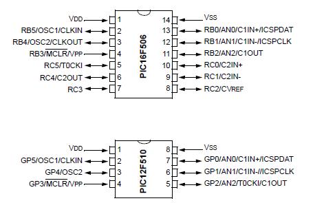
Pinout

  Connection Diagram


Specifications

Absolute Maximum Ratings†
Ambient temperature under bias............................... -40°C to +125°C
Storage temperature ............................................... -65°C to +150°C
Voltage on VDD with respect to VSS ...................................... 0 to +7.0V
Voltage on MCLR with respect to VSS.....................................0 to +14V
Voltage on all other pins with respect to VSS ......-0.3V to (VDD + 0.3V)
Total power dissipation(1) ......................................................700 mW
Max. current out of VSS pin .......................................................200 mA
Max. current into VDD pin ..........................................................150 mA
Input clamp current, IIK (VI < 0 or VI > VDD)............................±20 mA
Output clamp current, IOK (VO < 0 or VO > VDD).......................±20 mA
Max. output current sunk by any I/O pin .....................................25 mA
Max. output current sourced by any I/O pin .................................25 mA
Max. output current sourced by I/O port ....................................100 mA
Max. output current sunk by I/O port ..........................................100 mA

Note 1: Power dissipation is calculated as follows: PDIS = VDD x {IDD - IOH} + {(VDD-VOH) x IOH} + (VOL x IOL)
†NOTICE: Stresses above those listed under "Absolute Maximum Ratings" may cause permanent damage to the
device. This is a stress rating only and functional operation of the device at those or any other conditions above
those indicated in the operation listings of this specification is not implied. Exposure to maximum rating conditions
for extended periods may affect device reliability.


Customers Who Bought This Item Also Bought

Margin,quality,low-cost products with low minimum orders. Secure your online payments with SeekIC Buyer Protection.
Prototyping Products
DE1
Test Equipment
Fans, Thermal Management
Industrial Controls, Meters
Crystals and Oscillators
Static Control, ESD, Clean Room Products
View more