PI90LV180

Features: • Signaling Rates >660 Mbps (330 MHz)• Single 3.3V Power Supply Design• Driver:- ±350mV Differential Swing into a 100-Ohm load- Propogation Delay of 1.5ns Typ.- Low Voltage TTL (LVTTL) Inputs are 5V Tolerant- Driver is High Impedance when Disabled or VCC <1.5VR...

product image

PI90LV180 Picture
SeekIC No. : 004461463 Detail

PI90LV180: Features: • Signaling Rates >660 Mbps (330 MHz)• Single 3.3V Power Supply Design• Driver:- ±350mV Differential Swing into a 100-Ohm load- Propogation Delay of 1.5ns Typ.- Low Vo...

floor Price/Ceiling Price

Part Number:
PI90LV180
Supply Ability:
5000

Price Break

  • Qty
  • 1~5000
  • Unit Price
  • Negotiable
  • Processing time
  • 15 Days
Total Cost: $ 0.00

SeekIC Buyer Protection PLUS - newly updated for 2013!

  • Escrow Protection.
  • Guaranteed refunds.
  • Secure payments.
  • Learn more >>

Month Sales

268 Transactions

Rating

evaluate  (4.8 stars)

Upload time: 2025/1/10

Payment Methods

All payment methods are secure and covered by SeekIC Buyer Protection PLUS.

Notice: When you place an order, your payment is made to SeekIC and not to your seller. SeekIC only pays the seller after confirming you have received your order. We will also never share your payment details with your seller.
Product Details

Description


Features:

• Signaling Rates >660 Mbps (330 MHz)
• Single 3.3V Power Supply Design
• Driver:- ±350mV Differential Swing into a 100-Ohm load- Propogation Delay of 1.5ns Typ.- Low Voltage TTL (LVTTL) Inputs are 5V Tolerant- Driver is High Impedance when Disabled or VCC <1.5V
• Receiver:- Accepts ±50mV (min.) Differential Swing with up to 2.0Vground potential difference- Propagation Delay of 3.3ns Typ.- Low Voltage TTL (LVTTL) Outputs- Open, Short, and Terminated Fail Safe
• Industrial Temperature Operating Range: 40°C to 85°C
• Package Options: SOIC, TSSOP, MSOP
• Meets or Exceeds IEEE 1596.3 SCI Standard
• Meets or Exceeds ANSI/TIA/EIA-644 LVDS Standard
• Bus-Terminal ESD exceeds 12kV


Application

Applications include point-to-point and multidrop baseband datatransmission over a controlled impedance media of approximately100 ohms. These include intra-system connections via printedcircuit board traces or cables, hubs and routers for data communications;PBXs, switches, repeaters and base stations for telecommunicationsand other applications such as digital cameras, printersand copiers.


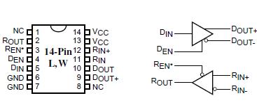
Pinout

  Connection Diagram


Specifications

Supply Voltage (VCC) ....................................................0.5V to +4.0V
Driver
Input Voltage (DIN) ....................................... 0.3V to (Vcc + 0.3V)
Output Voltage (DOUT+, DOUT-) ...............................0.3V to +3.9V
Short Circuit Duration (DOUT+, DOUT-) ......................... Continuous
Enable Input Voltage (DEN) ............................ 0.3V to (VCC + 0.3V)
Receiver
Input Voltage (RIN+, RIN-) ........................................ 0.3V to +3.9V)
Output Voltage (ROUT) ................................... 0.3V to (VCC + 0.3V)
Enable Input Voltage (REN*) ........................... 0.3V to (VCC + 0.3V)
Storage Temperature Range .................................. 65°C to +150°C
Lead Temperature Range Soldering (4s) ...............................+260°C
Maximum Junction Temperature ............................................+150°C
ESD Rating ............................................................................... >12kV


Description

The PI90LV179, PI90LV180, PI90LV050, and PI90LV051 are differentialline drivers and receivers (transceivers) that are compliant withthe IEEE 1596.3 SCI and ANSI/TIA/EIA-644 LVDS standards. PI90LV179, PI90LV180, PI90LV050, and PI90LV051 use low-voltage differential signaling (LVDS) to achievedata rates in excess of 660 Mbps while being less susceptible to noisethan single-ended transmission.

The drivers translate a low-voltage TTL/CMOS input into a lowvoltage(350mV typical) differential output signal. The receiverstranslate a differential 350mV input signal to a 3V CMOS output level.

The driver section can be independently set to a power-down andhigh-impedance output mode with the DEN pin (active HIGH). Thereceiver section is controlled by the REN* pin (active LOW).


Customers Who Bought This Item Also Bought

Margin,quality,low-cost products with low minimum orders. Secure your online payments with SeekIC Buyer Protection.
Resistors
Undefined Category
Hardware, Fasteners, Accessories
Connectors, Interconnects
View more