PI90LV022

Features: • Meets or Exceeds the Requirements of ANSI TIA/EIA-644-1995• Designed for Signaling Rates up to 650 Mbit/s (325 MHz)• Operates from a 3.3V Supply: 40°C to +85°C• Low Voltage Differential Signaling with Output Voltagesof ±350mV into:- 100 Ohm load (PI90LV022)- 50 ...

product image

PI90LV022 Picture
SeekIC No. : 004461450 Detail

PI90LV022: Features: • Meets or Exceeds the Requirements of ANSI TIA/EIA-644-1995• Designed for Signaling Rates up to 650 Mbit/s (325 MHz)• Operates from a 3.3V Supply: 40°C to +85°C• L...

floor Price/Ceiling Price

Part Number:
PI90LV022
Supply Ability:
5000

Price Break

  • Qty
  • 1~5000
  • Unit Price
  • Negotiable
  • Processing time
  • 15 Days
Total Cost: $ 0.00

SeekIC Buyer Protection PLUS - newly updated for 2013!

  • Escrow Protection.
  • Guaranteed refunds.
  • Secure payments.
  • Learn more >>

Month Sales

268 Transactions

Rating

evaluate  (4.8 stars)

Upload time: 2025/1/10

Payment Methods

All payment methods are secure and covered by SeekIC Buyer Protection PLUS.

Notice: When you place an order, your payment is made to SeekIC and not to your seller. SeekIC only pays the seller after confirming you have received your order. We will also never share your payment details with your seller.
Product Details

Description


Features:

• Meets or Exceeds the Requirements of ANSI TIA/EIA-644-1995
• Designed for Signaling Rates up to 650 Mbit/s (325 MHz)
• Operates from a 3.3V Supply: 40°C to +85°C
• Low Voltage Differential Signaling with Output Voltagesof ±350mV into:- 100 Ohm load (PI90LV022)- 50 Ohm load Bus LVDS Signaling (PI90LVB022)
• Accepts ±350mV differential inputs
• Wide common mode input voltage range: 0.2V to 2.7V
• Output drivers are high impedance when disabled orhen VCC 1.5V
• Inputs are open, short, and terminated fail safe
• Propagation Delay Time: 3.5ns
• ESD protection is 10kV on bus pins
• Bus Pins are High Impedance when disabled orwith VCC less than 1.5V
• TTL Inputs are 5V I/O Tolerant
• Power Dissipation at 400Mbit/s less than 150mW
• Industrial temperature rating
• Packaging (Pb-free & Green available):- 16-pin SOIC (W)- 16-pin TSSOP (L)


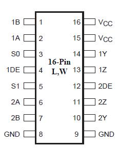
Pinout

  Connection Diagram


Specifications

Supply Voltage Range, VCC(1) ............................................................................... 0.5V to 4V
Voltage Range (DE, S0, S1) ...................................................................... 0.5 to 6V
Input Voltage Range, VI (A or B) ............................................ 0.5V to VCC + 0.5V
Electrostatic Discharge: A, B, Y, Z, and GND(2) ................ Class 3, A: 16kV, B:600V
All Pins ............................................ Class 3, A: 7kV, B:500V
Storage Temperature Range.............................................................. 65°C to 150°C
Lead Temperature 1, 6 mm (1/16 inch) from case for 10 seconds ................... 260°C

† Stresses beyond those listed under "Absolute Maximum Ratings" may cause permanentdamage to the device. These are stress ratings only, and functional operation of the deviceat these or any other conditions beyond those indicated under "Recommended OperatingConditions" is not implied. Exposure to Absolute-Maximum-Rated conditions for extendedperiods may affect device reliability.

Notes:
1. All voltage values, except differential I/O bus voltages, are with respect to ground terminal.

2. Tested in accordance with MIL-STD-883C Method 3015.7


Description

The PI90LV022 and PI90LVB022 are differential line drivers and receivers that use Low Voltage Differential Signaling (LVDS) to achieve signaling rates as high as 650 Mbps. The receiver outputs of PI90LV022 and PI90LVB022 can be switched to either or both drivers through the multiplexercontrol signals S0 and S1. PI90LV022 and PI90LVB022 allows the flexibility to performsplitter or signal routing functions with a single device.

The LVDS standard provides a minimum differential output voltagemagnitude of 247mV into a 100 Ohm load and receipt of 100mV DCsignals with up to 1V of ground potential difference between atransmitter and receiver. The PI90LVB022 doubles the output drieurrent to achieve Bus LVDS signaling levels with a 50 Ohm load.

A doubly terminated Bus LVDS line enables multi-point configurations.Switching between channels does not create false transitionson the outputs.

The intended application of PI90LV022 and PI90LVB022 and signaling techniqueis for both point-to-point base-band (PI90LV022) and multipoint(PI90LVB022) data transmissions over controlled impedance media.


Customers Who Bought This Item Also Bought

Margin,quality,low-cost products with low minimum orders. Secure your online payments with SeekIC Buyer Protection.
Hardware, Fasteners, Accessories
Programmers, Development Systems
Boxes, Enclosures, Racks
Connectors, Interconnects
Computers, Office - Components, Accessories
View more