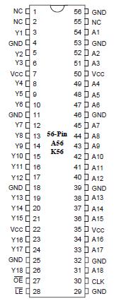
Features: · Very high-speed, low-noise universal bus driver with embedded resistor outputs
· Meets PC133 SDRAM Registered DIMM specification
· Implements output impedance control for low-noise and heavy-load applications
· Fast Propagation Delay: 2.5ns max. for 50pF test load
· VCC = 3.3V or 2.5V or 1.8V
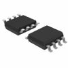
· Packages available: - 56-pin 240 mil wide plastic TSSOP (A) - 56-pin 173 mil wide plastic TVSOP (K)Pinout Specifications
Storage Temperature ............................................................................................................. –65°C to +150°C
Ambient Temperature with Power Applied ............................................................................ –40°C to +85°C
Supply Voltage Range, VCC ...................................................................................... –0.5V to +4.6V
Input Voltage Range, VI
(1) ........................................................................................................................... –0.5V to +4.6V
Voltage range applied to any output in the high-impedance or power-off state, VO(1) ........... –0.5V to +4.6V
Voltage range applied to any output in the high or low state, VO(1,2) ............................... –0.5V to VCC +0.5V
Input clamp current, IIK (VI <0) .................................................................................................... –50mA
Output clamp current, IOK (VO <0) ............................................................................................... –50mA
Continuous output current, IO ...................................................................................................... ±50mA
Continuous current through each VCC or GND............................................................................±100mA
Package thermal impedance, qJA
(3): A (TSSOP) package ....................................................................81°C/W
K (TVSOP) package ....................................................................86°C/W
Note:
1. Input and output negative voltage ratings may be exceeded if the input and output current ratings are observed.
2. Output positive voltage rating may be exceeded up to 4.6V maximum if the output current rating is observed.
3. Package thermal impedance is calculated in accordance with JESD 51.
Stresses greater than those listed under MAXIMUM RATINGS may cause permanent damage to the device. This is a stress rating only and functional operation of the device at these or any other conditions above those ndicated in the operational sections of this specification is not implied. Exposure to absolute maximum rating conditions for extended periods may affect reliability.
DescriptionPericom Semiconductor's PI74AVC series of logic circuits are produced using the Company's advanced 0.35 micron CMOS technology, achieving industry leading speed. The 18-bit PI74AVC16834 universal bus driver is designed for 1.8V to 3.6V VCC operation.
Data flow from A to Y is controlled by Output Enable (OE). The PI74AVC16834 operates in the transparent mode when LE is LOW. The A data is latched if CLK is held at a high or low logic level. If LE is HIGH, the A-bus is stored in the latch/flip-flop on the low-to-high transition of CLK. When OE is HIGH, the outputs of PI74AVC16834 are in the highimpedance state.
The PI74AVC16834 bus driver is designed to drive an array of 133 MHz synchronous memory chips, with minimal undershoot/ overshoot noise, and to meet the input signal rise/fall time requirement of memory chips.
The output drivers of PI74AVC16834 have an embedded series-resistor.
For DIMM module design, no external series termination resistors near the buffer drivers or any other termination resistors are required. PI74AVC16834 feature simplifies DIMM module layout design, and results in cost savings.

 PI74AVC16834 Data Sheet


