Features: · PI74ALVCH16271 is designed for low voltage operation, VCC = 2.3V to 3.6V· Hysteresis on all inputs· Typical VOLP (Output Ground Bounce) < 0.8V at VCC = 3.3V, TA = 25°C · Typical VOHV (Output VOH Undershoot) < 2.0V at VCC = 3.3V, TA = 25°C· Bus Hold retains last active bus state d...
PI74ALVCH16271: Features: · PI74ALVCH16271 is designed for low voltage operation, VCC = 2.3V to 3.6V· Hysteresis on all inputs· Typical VOLP (Output Ground Bounce) < 0.8V at VCC = 3.3V, TA = 25°C · Typical VOHV ...
SeekIC Buyer Protection PLUS - newly updated for 2013!
268 Transactions
All payment methods are secure and covered by SeekIC Buyer Protection PLUS.
Features: SpecificationsDescriptionPericom Semiconductor's PI74ALPTX series of logic circuits are ...
Features: • PI74ALVC162334 is designed for low voltage operation, VCC = 2.3V to 3.6V• ...
Features: · PI74ALVC162834 is designed for low voltage operation, VCC = 2.3V to 3.6V· Outputs have...
· PI74ALVCH16271 is designed for low voltage operation, VCC = 2.3V to 3.6V
· Hysteresis on all inputs
· Typical VOLP (Output Ground Bounce) < 0.8V at VCC = 3.3V, TA = 25°C
· Typical VOHV (Output VOH Undershoot) < 2.0V at VCC = 3.3V, TA = 25°C
· Bus Hold retains last active bus state during 3-State, eliminating the need for external pullup resistors
· Industrial operation at 40°C to +85°C
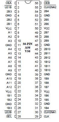
· Packages available: - 56-pin 240 mil wide plastic TSSOP (A56) - 56-pin 300 mil wide plastic SSOP (V56)
Pericom Semiconductor's PI74AVC series of logic circuits are produced using the Company's advanced 0.35 micron CMOS technology, achieving industry leading speed. This 12-bit to 24-bit multiplexed bus exchanger is designed for 2.3V to 3.6V VCC operation.
The PI74ALVCH16271 is intended for applications in which two separate data paths must be multiplexed onto, or demultiplexed from, a single data path. PI74ALVCH16271 is particularly suitable as an interface between conventional DRAMs and high-speed microprocessors Data is stored in the internal A-to-B registers on the low-to-high transition of the clock (CLK) input, provided clock-enable (CLKENA) inputs are low. Proper control of these inputs allows two sequential 12-bit words to be presented as a 24-bit word on the B port.
To maximize memory access throughput, transparent latches in the B-to-A path allow asynchronous operation. These latches transfer data when the latch-enable (LE) inputs are low. The select (SEL) line selects 1B or 2B data for the A outputs. Data flow is controlled by the active-low output enables (OEA, OEB).
To ensure the high-impedance state during power up or power down, OE should be tied to VCC through a pullup resistor, the minimum value of the resistor is determined by the current-sinking capability of the driver.
Active bus-hold circuitry of PI74ALVCH16271 is provided to hold unused or floating data inputs at a valid logic level.