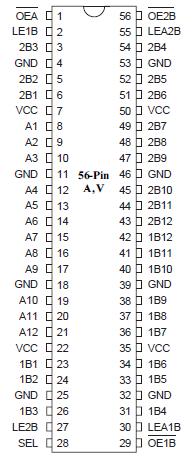
Features: · PI74ALVCH16260 is designed for low voltage operation
· VCC = 2.3V to 3.6V
· Hysteresis on all inputs
· Typical VOLP (Output Ground Bounce)< 0.8V at VCC = 3.3V, TA = 25°C
· Typical VOHV (Output VOH Undershoot) 2.0V at VCC = 3.3V, TA = 25°C
· Bus Hold retains last active bus state during 3-State,eliminating the need for external pullup resistors
· Industrial operation at –40°C to +85°C
· Packages available:-56-pin 240 mil wide plastic TSSOP (A) -56-pin 300 mil wide plastic SSOP (V)Pinout Specifications
Storage Temperature .................................................................... 65°C to +150°C
Ambient Temperature with Power Applied .................................... 40°C to +85°C
Supply Voltage to Ground Potential (Inputs & Vcc Only) .............. 0.5V to +7.0V
Supply Voltage to Ground Potential (Outputs & D/O Only) ........... 0.5V to +7.0V
DC Input Voltage ............................................................................ 0.5V to +7.0V
DC Output Current ..................................................................................... 120 mA
Power Dissipation ..........................................................................................1.0W
Note:
Stresses greater than those listed under MAXIMUM RATINGS may cause permanent damage to the device. This is a stress rating only and functional operation of the device at these or any other conditions above those indicated in the operational sections of this specification is not implied. Exposure to absolute maximum rating conditions for extended periods may affect reliability.
DescriptionPericom Semiconductor's PI74ALVCH series of logic circuits areproduced using the Company's advanced 0.5 micron CMOStechnology, achieving industry leading speed.
The PI74ALVCH16260 is a 12-bit to 24-bit multiplexed D-type latchesigned for 2.3V to 3.6 VCC operation. PI74ALVCH16260 is used in applicationswhere two separate datapaths must be multiplexed onto, ordemultiplexed from, a single data path.
PI74ALVCH16260 applications include multiplexing and/or demultiplexingaddress and data information in microprocessor or bus-interfaceand in memory-interleaving.
Three 12-bit I/O ports (A1-A12, 1B1-1B12, and 2B1-2B12) are availablefor address and/or data transfer. The output-enable (OE1B, OE2B,and OEA) inputs control bus transceiver functions. The OE1B andOE2B control signals also allow bank control in the A-to-B direction.Address and/or data information can be stored using the internalstorage latches. The latch-enable (LE1B, LE2B, LEA1B, and LEA2B)inputs of PI74ALVCH16260 are used to control data storage. When the latch-enable inputis HIGH, the latch is transparent. When the latch-enable input goesLOW, the data present at the inputs is latched and remains latcheduntil the latch-enable input is returned HIGH.
To ensure high-impedance state during power up or power down,OE should be tied to VCC through a pullup resistor whose minimumvalue is determined by the current-sinking capability of the driver.
Active bus-hold circuitry is provided to hold unused or floating ata inputs at a valid logic level.

 PI74ALVCH16260 Data Sheet


