Features: ` PI74ALVCH162268 is designed for low voltage operationVCC = 2.3V to 3.6V
` Hysteresis on all inputs
` Typical VOLP (Output Ground Bounce)< 0.8V at VCC = 3.3V, TA = 25°C
` Typical VOHV (Output VOH Undershoot)< 2.0V at VCC = 3.3V, TA = 25°C
` B-port outputs have equivalent 26W series resistors,no external resistors are required.
` Bus Hold retains last active bus state during 3-stateeliminates the need for external pullup resistors
` Industrial operation at 40°C to +85°C
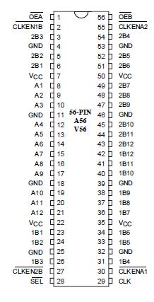
` Packages available: 56-pin 240 mil wide plastic TSSOP (A56) 56-pin 300 mil wide plastic SSOP (V56)
Pinout Specifications
Storage Temperature .................................................. –65°C to +150°C
Supply Voltage Range, VCC ........................................... –0.5V to 4.6V
Input Voltage Range,VI :
Except I/O ports (See Note 1): ........................................ –0.5V to 4.6V
I/O ports (See Notes 1 and 2) .............................. –0.5V to VCC + 0.5V
Output Voltage Range, VO (See Notes 1and 2) .. –0.5V to VCC + 0.5V
Input Clamp current, IIK (VI < 0) .............................................. –50mA
Output Clamp current, IOK (VO < 0 or VO > VCC) ...................±50mA
Continous Output Current, IO (VO = 0 to VCC) ........................±50mA
Continous Current through each VCC or GND ........................±100mA
Maximum Power Dissipation:
A package ................................................................... 1W
V package ................................................................ 1.4W
Note:
Stresses greater than those listed under MAXIMUMRATINGS may cause permanent damage to the device.This is a stress rating only and functional operation of thedevice at these or any other conditions above thoseindicated in the operational sections of this specificationis not implied. Exposure to absolute maximum rating onditions for extended periods may affect reliability.
DescriptionPericom Semiconductor's PI74ALVCH series of logic circuits areproduced in the Company's advanced 0.5 micron CMOStechnology, achieving industry leading speed.
This 12-bit to 24-bit registered bus exchanger PI74ALVCH162268 is designed for 2.3Vo 3.6V Vcc operation.
The PI74ALVCH162268 is used for applications in which datamust be transferred from a narrow high-speed bus to a wide, lowerfrequency bus.
The PI74ALVCH162268 provides synchronous data exchange between the twoports. Data is stored in the internal registers on the low-to-hightransition of the clock (CLK) input when the appropriate clockenable (CLKEN) inputs are low. The select (SEL) line issynchronous with CLK and selects 1B or 2B input data for the Aoutputs.
For data transfer in the A-to-B direction, a two stage pipeline isprovided in the A-to-1B path, with a single storage register in theA-to-2B path. Proper control of these inputs allows two sequential12-bit words to be presented synchronously as a 24-bit word on theB-port. Data flow of PI74ALVCH162268 is controlled by the active-low output enables(OEA, OEB). These control terminals are registered so bus directionchanges are synchronous with CLK.
The B outputs, PI74ALVCH162268 is designed to sink up to 12mA, includeequivalent 26W resistors to reduce overshoot and undershoot.
To ensure the high-impedance state during power up or power own, a clock pulse should be applied as soon as possible and OE hould be tied to VCC through a pullup resistor, the minimum valueof the resistor PI74ALVCH162268 is determined by the current-sinking capability ofthe driver. Because OE is being routed through a register, theactive state of the outputs cannot be determined prior to the arrivalof the first clock pulse.
Active bus-hold circuitry of PI74ALVCH162268 is provided to hold unused or floatingdata inputs at a valid logic level.

 PI74ALVCH162268 Data Sheet


