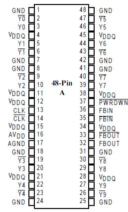
Features: • PLL clock distribution optimized for DDR2 SDRAM applications.
• Distributes one differential clock input pair to ten differential clock output pairs.
• Differential Inputs (CLK, CLK) and (FBIN, FBINFBIN)
• Input OE/OS: LVCMOS
• Differential Outputs (Y[0:9], Y[0:9] and (FBOUT, FBOUT)
• External feedback pins (FBIN, FBIN) are used tosynchronize the outputs to the clock input.
• Operates at AVDD = 1.8V for core circuit and internal PLL, and VDDQ = 1.8V for differential output drivers
• Available Packages: Plastic 48-pin TSSOPPinout Specifications
|
Symbol |
Parameter |
Min. |
Max. |
Units |
|
VCC,AVDD |
I/O supply voltage range and analog /core supply voltage range |
-0.5 |
3.6 |
V |
|
VI |
Input voltage range |
-0.5 |
VDDQ +0.5 |
|
VO |
Output voltage range |
-0.5 |
|
TSTG |
Storage temperature |
-65 |
150 |
|
Note: Stress beyond those listed under "Absolute Maximum Ratings" may cause permanent damage to the device.DescriptionPI6CU877 PLL clock driver is developed for Registered DDR2 DIMM applications with 1.8V operation and differential data input and output levels.
The PI6CU877 is a zero delay buffer that distributes a differential clock input pair (CLK, CLK) to eleven differential pairs of clock outputs which includes feedback clock (Y[0:9], Y[0:9]; FBOUT, FBOUT).
The clock outputs of PI6CU877 are controlled by CLK/CLK, FBOUT, FBOUT, the LVCMOS (OE, OS) and the Analog Power input (AVDD). When OE is LOW the outputs except FBOUT, FBOUT, are disabled while the internal PLL continues to maintain its locked-in frequency. OS is a program pin that must be tied to GND or VDD. When OS is high, OE will function as described above. When OS is LOW, OE has no effect on Y7/Y7, PI6CU877 is free running. When AVDD is grounded, the PLL is turned off and bypassed for test purposes.
When CLK/CLK are logic low, the PI6CU877 will enter a low power mode. An input logic detection circuit will detect the logic low level and perform a low power state where all Y[0:9], Y[0:9]; FBOUT, FBOUT, and PLL are OFF.
PI6CU877 is a high performance, low skew, and low jitter PLL clock driver, and it is also able to track Spread Spectrum Clocking (SSC) for reduced EMI.

 PI6CV857L Data Sheet


