PI6C48535-01

Features: • Maximum operation frequency: 500 MHz• 4 pair of differential LVPECL outputs• Selectable CLK0 and CLK1 inputs• CLK0, CLK1 accept LVCMOS, LVTTL input level• Output Skew: 80ps (maximum)• Part-to-part skew: 150ps (maximum)• Propagation delay: 1.9ns...

product image

PI6C48535-01 Picture
SeekIC No. : 004461202 Detail

PI6C48535-01: Features: • Maximum operation frequency: 500 MHz• 4 pair of differential LVPECL outputs• Selectable CLK0 and CLK1 inputs• CLK0, CLK1 accept LVCMOS, LVTTL input level• O...

floor Price/Ceiling Price

Part Number:
PI6C48535-01
Supply Ability:
5000

Price Break

  • Qty
  • 1~5000
  • Unit Price
  • Negotiable
  • Processing time
  • 15 Days
Total Cost: $ 0.00

SeekIC Buyer Protection PLUS - newly updated for 2013!

  • Escrow Protection.
  • Guaranteed refunds.
  • Secure payments.
  • Learn more >>

Month Sales

268 Transactions

Rating

evaluate  (4.8 stars)

Upload time: 2024/11/25

Payment Methods

All payment methods are secure and covered by SeekIC Buyer Protection PLUS.

Notice: When you place an order, your payment is made to SeekIC and not to your seller. SeekIC only pays the seller after confirming you have received your order. We will also never share your payment details with your seller.
Product Details

Description


Features:

• Maximum operation frequency: 500 MHz
• 4 pair of differential LVPECL outputs
• Selectable CLK0 and CLK1 inputs
• CLK0, CLK1 accept LVCMOS, LVTTL input level
• Output Skew: 80ps (maximum)
• Part-to-part skew: 150ps (maximum)
• Propagation delay: 1.9ns (maximum)
• 3.3V power supply
• Pin-to-pin compatible to ICS8535-01
• Operating Temperature: -40oC to 85oC
• Packaging (Pb-free & Green available): - 20-pin TSSOP (L)


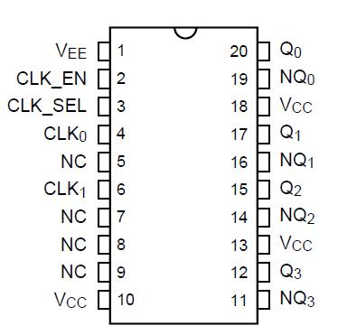
Pinout

  Connection Diagram


Specifications

Product Specs: Voltage: 3.3V Function: Buffer, Driver Jitter: - Skew: 30ps Speed: 500MHz I/O: TTL/CMOS/PECL Temp: Ind Outputs: 4 Pins: 20 Packages: TSSOP (L20) Pb-Free and Green: Yes - more info RoHS Material Declarations: PI6C48535-01LE MDR (pdf)

Symbol Parameter Conditions Min. Typ. Max. Units
VCC Supply voltage Referenced to GND 4.6 V
VIN Input voltage Referenced to GND -0.5 VCC+0.5V
VOUT Output voltage Referenced to GND -0.5 VCC+0.5V
TSTG Storage temperature -65 150 °C

Notes:
1. Stresses above those listed under Absolute Maximum Ratings may cause permanent damage to the device. These ratings are stress speci fications only and correct functional operation of the device at these or any other conditions above those listed in the operational sections of the specifications is not implied. Exposure to absolute maximum rating conditions for extended periods may affect product reliability.


Description

PI6C48535-01 3.3V, 4 Outputs, LVTTL/LVCMOS to LVPECL Clock Buffer with Selectable inputs

The PI6C48535-01 is a high-performance low-skew LVPECL fanout buffer. PI6C48535-01 features two selectable single-ended clock inputs and translates to four LVPECL outputs. The CLK0 and CLK1 inputs accept LVCMOS or LVTTL signals. The outputs are synchronized with input clock during asynchronous assertion/deassertion of CLK_EN pin. PI6C48535-01 is ideal for single-ended LVTTL/LVCMOS to LVPECL translations. Typical clock translation and distribution applications are data-communications and telecommunications.


Customers Who Bought This Item Also Bought

Margin,quality,low-cost products with low minimum orders. Secure your online payments with SeekIC Buyer Protection.
Cables, Wires
Transformers
Fans, Thermal Management
Resistors
Boxes, Enclosures, Racks
View more