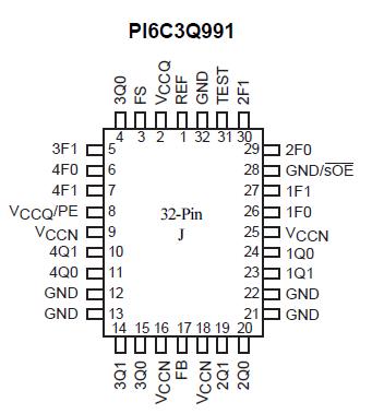
Features: · PI6C3Q99X family provides following products: PI6C3Q991: 32-pin PLCC version PI6C3Q993: 28-pin QSOP version· Inputs are 5V I/O Tolerant· 4 pairs of programmable skew outputs· Low skew: 200ps same pair; 250ps all outputs· Selectable positive or negative edge synchronization: Excellent f...
PI6C3Q991: Features: · PI6C3Q99X family provides following products: PI6C3Q991: 32-pin PLCC version PI6C3Q993: 28-pin QSOP version· Inputs are 5V I/O Tolerant· 4 pairs of programmable skew outputs· Low skew: 2...
SeekIC Buyer Protection PLUS - newly updated for 2013!
268 Transactions
All payment methods are secure and covered by SeekIC Buyer Protection PLUS.
Supply Voltage to ground ........................................................ 0.5V to 7.0V
DC input Voltage VI .................................................................... 0.5V to VCC + 0.5V
Maximum Power Dissipation at TA = 85°C, PLCC ......................... 0.80 watts
QSOP ....................... 0.66 watts
TSTG Storage temperature ....................................................65°C to 150°C
Stresses above those listed under Absolute Maximum Ratings may cause permanent damage to the device. These ratings are stress specifications only and functional operation of the device at these or any other conditions above those listed in the operational sections of the specifications is not implied. Exposure to absolute maximum rating conditions for extended periods may affect product reliability.
The PI6C3Q99X family is a high fanout 3.3V PLL-based clock driver intended for high performance computing and data-communications applications. A key feature of the programmable skew is the ability of outputs to lead or lag the REF input signal. The PI6C3Q991 has 8 programmable skew outputs in 4 banks of 2, while the PI6C3Q993 has 6 programmable skew outputs and 2 zero skew outputs. Skew is controlled by 3-level input signals that may be hardwired to appropriate HIGH-MID-LOW levels.
When the GND/sOE pin is held low, all the outputs are synchronously enabled. However, if GND/sOE is held high, all the outputs except 3Q0 and 3Q1 are synchronously disabled. Furthermore, when the V CCQ /PE is held high, all the outputs are synchronized with the positive edge of the REF clock input. When VCCQ /PE is held low, all the outputs are synchronized with the negative edge of REF. Both devices have LVTTL outputs with 12mA balanced drive outputs.