PI6C2516

Features: · High Performance Phase-Locked Loop Clock Distribution for Synchronous DRAM, server and networking applications.· Zero Input-to-Output delay: Distribute One Clock Input to four banks of four outputs, with separate output enables for each bank.· Allow Clock Input to have Spread Spectrum ...

product image

PI6C2516 Picture
SeekIC No. : 004461175 Detail

PI6C2516: Features: · High Performance Phase-Locked Loop Clock Distribution for Synchronous DRAM, server and networking applications.· Zero Input-to-Output delay: Distribute One Clock Input to four banks of f...

floor Price/Ceiling Price

Part Number:
PI6C2516
Supply Ability:
5000

Price Break

  • Qty
  • 1~5000
  • Unit Price
  • Negotiable
  • Processing time
  • 15 Days
Total Cost: $ 0.00

SeekIC Buyer Protection PLUS - newly updated for 2013!

  • Escrow Protection.
  • Guaranteed refunds.
  • Secure payments.
  • Learn more >>

Month Sales

268 Transactions

Rating

evaluate  (4.8 stars)

Upload time: 2025/1/10

Payment Methods

All payment methods are secure and covered by SeekIC Buyer Protection PLUS.

Notice: When you place an order, your payment is made to SeekIC and not to your seller. SeekIC only pays the seller after confirming you have received your order. We will also never share your payment details with your seller.
Product Details

Description


Features:

· High Performance Phase-Locked Loop Clock Distribution for Synchronous DRAM, server and networking applications.
· Zero Input-to-Output delay: Distribute One Clock Input to four banks of four outputs, with separate output enables for each bank.
· Allow Clock Input to have Spread Spectrum modulation for EMI reduction. The clock outputs track the Clock Input modulation.
· Maximum clock frequency of 150 MHz.
· Low jitter: Cycle-to-Cycle jitter ±100ps max
· Operates at 3.3V VCC
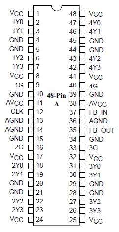
· Available Packaging: - 48-pin TSSOP (Thin Shrink Small Outline) (A)


Pinout

  Connection Diagram


Specifications

Symbol
Parameter
Min.
Max.
Units
VCC
Supply voltage range
-0.5
4.5
V
VI
Input voltage range(1)
-0.5
6.5
VO
Output voltage range(1,2)
-0.5
VCC + 0.5
VIK
Input Clamp Current
-50
 
mA
IO_DC
Continuous output current (VO = 0 or VCC)  
±50
IO_DC
Continuous output through VCC or ground
±100
Power
Maximum power dissipation at TA= 55 in still air(3)
0.85
W
TSTG
Storage temperature
-65
150

* Stresses beyond those listed under “Absolute Maximum Ratings” may cause permanent damage to the device. This is a stress ratings only and functional operation of the device at these or any other conditions beyond those indicated under “recommended operating conditions” is not implied. Exposure to absolute-maximum-rat d conditions for extended periods may affect reliability.

Notes:
1. The input and output negative-voltage ratings may be exceeded if the input and output clamp-current ratings are observed.
2. This value is limited to 4.6V maximum.
3. Maximum package power dissipation is calculated using a junction temperature of 150°C and a board trace length of 750 mils.


Description

The PI6C2516 family is a low-skew, low jitter, phase-locked loop (PLL) clock driver, distributing high-frequency clock signals for SDRAM, server and networking applications. By connecting the feedback FB_OUT output to the feedback FB_IN input, the propagation delay from the CLK input to any clock output will be nearly zero. This zero-delay feature of PI6C2516 allows the CLK input clock to be distributed, providing 4 banks of four outputs.

For test purposes, the PLL can be bypassed by strapping the AVCC to ground.

The PI6C2516 family has the same pinout as the TI CDC2516, with the added feature of allowing Spread Spectrum clock input.


Customers Who Bought This Item Also Bought

Margin,quality,low-cost products with low minimum orders. Secure your online payments with SeekIC Buyer Protection.
Static Control, ESD, Clean Room Products
Semiconductor Modules
Isolators
Inductors, Coils, Chokes
View more