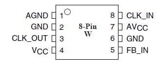
Features: • High-Performance, Phase-Locked-Loop Clock Driver and zerodelay buffer
• Allows Clock Input to have Spread Spectrum modulation for EMI reduction
• Zero Input-to-Output delay
• Low jitter: Cycle-to-Cycle jitter ±75ps max.
• On-chip series damping resistor at clock output drivers for low noise and EMI reduction
• Operates at 3.3V VCC
• Wide range of Clock Frequencies 80 to 134 MHz
• Package: Plastic 8-pin 150-mil SOIC (W) Plastic 8-pin 150-mil SOIC (WE) Pb-free
ApplicationIf a system designer needs more than 16 outputs with the features just described, using two or more zero-delay buffers, such as the PI6C2509Q, or PI6C2510Q, is likely to be impractical. The device-to-device skew introduced can significantly reduce the performance. Pericom recommends using a zero-delay buffer and an eighteen output non-zero-delay buffer. As shown in Figure 1, this combination produces a zero-delay buffer with all the signal characteristics of the original zero-delay buffer, but with as many outputs as the non-zero-delay buffer part. For example, when combined with an eighteen output non-zero delay buffer, a system designer can create a seventeen-output zero-delay buffer.
Pinout Specifications
|
Symbol |
Parameter |
Min. |
Max. |
Units |
|
VI |
Input voltage range |
-0.5 |
VCC + 0.5 |
V |
|
VO |
Output voltage range |
|
VI_DC |
DC input voltage |
3.8 |
|
IO_DC |
DC output current |
|
100 |
mA |
|
Power |
Maximum power dissipation at TA= 55 in still air |
|
1.0 |
W |
|
TSTG |
Storage temperature |
-65 |
150 |
|
Note:
1. Stress beyond those listed under "absolute maximum ratings" may cause permanent damage to the device.DescriptionThe PI6C2501A features a low-skew, low-jitter, phase-locked loop (PLL) clock driver. By connecting the CLK_OUT output to the feedback FB_IN input, the propagation delay from the CLK_IN input to CLK_OUT output will be nearly zero.

 PI6C2501A Data Sheet


