PI6C2409

Features: • Maximum rated frequency: 133 MHz• Low cycle-to-cycle jitter• Input to output delay, less than 200ps• Internal feedback allows outputs to be synchronized to the clock input• Operates at 3.3V VDD• Space-saving Packages: 150-mil SOIC (W) 173-mil TSSOP (...

product image

PI6C2409 Picture
SeekIC No. : 004461160 Detail

PI6C2409: Features: • Maximum rated frequency: 133 MHz• Low cycle-to-cycle jitter• Input to output delay, less than 200ps• Internal feedback allows outputs to be synchronized to the cl...

floor Price/Ceiling Price

Part Number:
PI6C2409
Supply Ability:
5000

Price Break

  • Qty
  • 1~5000
  • Unit Price
  • Negotiable
  • Processing time
  • 15 Days
Total Cost: $ 0.00

SeekIC Buyer Protection PLUS - newly updated for 2013!

  • Escrow Protection.
  • Guaranteed refunds.
  • Secure payments.
  • Learn more >>

Month Sales

268 Transactions

Rating

evaluate  (4.8 stars)

Upload time: 2024/11/25

Payment Methods

All payment methods are secure and covered by SeekIC Buyer Protection PLUS.

Notice: When you place an order, your payment is made to SeekIC and not to your seller. SeekIC only pays the seller after confirming you have received your order. We will also never share your payment details with your seller.
Product Details

Description


Features:

• Maximum rated frequency: 133 MHz
• Low cycle-to-cycle jitter
• Input to output delay, less than 200ps
• Internal feedback allows outputs to be synchronized to the clock input
• Operates at 3.3V VDD
• Space-saving Packages: 150-mil SOIC (W) 173-mil TSSOP (L)


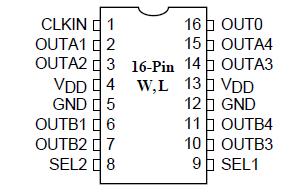
Pinout

  Connection Diagram


Specifications

Supply Voltage to Ground Potential ....................................................................................... 0.5V to +7.0V
DC Input Voltage (Except CLKIN) .......................................................................................   . 0.5V to VDD +0.5V
DC Input Voltage CLKIN ......................................................................................................... 0.5 to 7V
Storage Temperature ............................................................................................................. 65ºC to +150ºC
Maximum Soldering Temperature (10 seconds) ......................................................................... 260ºC
Junction Temperature ................................................................................................................ 150ºC
Static Discharge Voltage (per MIL-STD-883, Method 3015) ........................................................ >2000V


Description

The PI6C2409 is a PLL based, zero-delay buffer, with the ability to distribute nine outputs of up to 133MHz at 3.3V.

All the outputs are distributed from a single clock input CLKIN and output OUT0 performs zero delay by connecting a feedback to PLL. PI6C2409 has two banks of four outputs that can be controlled by the selection inputs, SEL1 & SEL2. It also has a powersparing feature: when input SEL1 is 0 and SEL2 is 1, PLL is turned off and all outputs are referenced from CLKIN. PI6C2409 is available in high drive and industrial environment versions.

An internal feedback on OUT0 is used to synchronize the outputs to the input; the relationship between loading of this signal and the outputs determines the input-output delay. PI6C2409 are characterized for both commercial and industrial operation


Customers Who Bought This Item Also Bought

Margin,quality,low-cost products with low minimum orders. Secure your online payments with SeekIC Buyer Protection.
Prototyping Products
DE1
Test Equipment
Motors, Solenoids, Driver Boards/Modules
Cables, Wires - Management
View more