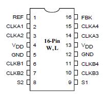
Features: · 10 MHz to 140 MHz operating range
· Zero input-output propagation delay, adjustable by capacitive load on FBK input
· Multiple configurations, see “Available PI6C2308A Configurations” table
· Input to output delay, less than 150ps
· Multiple low skew outputs - Output-output skew less than 200ps - Device-device skew less than 500ps - Two banks of four outputs, Hi-Z by two select inputs
· Low Jitter, less than 200ps
· 3.3V operation
· Available in industrial &commercial temperatures
· Packages: - Space-saving 16-pin, 150-mil SOIC (W) - 16-pin TSSOP (L)
Pinout SpecificationsSupply Voltage to Ground Potential ...................................................–0.5V to +7.0V
DC Input Voltage (Except REF) .................................................. –0.5V to VDD +0.5V
DC Input Voltage REF ................................................................................ –0.5 to 7V
Storage Temperature ........................................................................ –65ºC to +150ºC
Maximum Soldering Temperature (10 seconds) ................................................ 260ºC
Junction Temperature ....................................................................................... 150ºC
Static Discharge Voltage
(per MIL-STD-883, Method 3015) .................................................................. >2000VDescriptionProviding two banks of four outputs, the PI6C2308A is a 3.3V zerodelay buffer designed to distribute clock signals in applications including PC, workstation, datacom, telecom, and high-performance systems. Each bank of four outputs can be controlled by the select inputs as shown in the Select Input Decoding Table.
It provides 8 copies of a clock signal that has 150ps phase error compared to a reference clock. The skew between the output clock signals for PI6C2308A is less than 200ps. When there are no rising edges on the REF input, it enters a power down state. In this mode, the PLL is off and all outputs are Hi-Z. This results in less than 12mA of current draw. The Select Input Decoding table shows additional examples when the PLL shuts down. It configuration table shows all available devices.
The base part, PI6C2308A-1, provides output clocks in sync with a reference clock. With faster rise and fall times, the PI6C2308A-1H is the high-drive version of the PI6C2308A-1. Depending on which output drives the feedback pin, PI6C2308A-2 provides 2X and 1X clock signals on each output bank. The PI6C2308A-3 allows the user to obtain 4X and 2X frequencies on the outputs. The PI6C2308A-4 provides 2X clock signals on all outputs. It (-1, -2, -3, -4) allows bank B to be Hi-Z when all output clocks are not required.The PI6C2308A-6 allows bank B to switch from Reference clock to half of the frequency of Reference clock using the control inputs S1 and S2 if Bank A is connected to feedback FBK. In addition, using the control inputs S1 and S2, the PI6C2308A-6 allows bank A to switch from Reference clock to 2X the frequency of Reference clock if Bank B is connected to feedback FBK. For testing purposes, the select inputs connect the input clock directly to outputs.

 PI6C2308A Data Sheet


