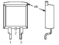
PinoutSpecifications SYMBOL PARAMETER CONDITIONS MIN. MAX. UNIT IDIDMPDD/TmbVGSEASIASTj, Tstg Continuous drain currentPulsed drain currentTotal dissipationLinear derating factorGate-source voltageSingle pulse avalancheenergyPeak avalanche currentOperating junction andstorage temperat...
PHB2N50: PinoutSpecifications SYMBOL PARAMETER CONDITIONS MIN. MAX. UNIT IDIDMPDD/TmbVGSEASIASTj, Tstg Continuous drain currentPulsed drain currentTotal dissipationLinear derating factorGate-so...
SeekIC Buyer Protection PLUS - newly updated for 2013!
268 Transactions
All payment methods are secure and covered by SeekIC Buyer Protection PLUS.
SYMBOL | PARAMETER | CONDITIONS | MIN. | MAX. | UNIT |
ID IDM PD D/Tmb VGS EAS IAS Tj, Tstg |
Continuous drain current Pulsed drain current Total dissipation Linear derating factor Gate-source voltage Single pulse avalanche energy Peak avalanche current Operating junction and storage temperature range |
Tmb = 25 ; VGS = 10 V Tmb = 100 ; VGS = 10 V Tmb = 25 Tmb = 25 Tmb > 25 VDD 50 V; starting Tj = 25; RGS = 50 ; VGS = 10 V VDD 50 V; starting Tj = 25; RGS = 50 ; VGS = 10 V |
- - - - - - - - - 55 |
2 1.3 8 50 0.4 ± 30 100 2 150 |
A A A W W/K V mJ A |
PHB2N50 N-channel enhancement mode field-effect power transistor in a plastic envelope suitable for surface mounting featuring high avalanche energy capability, stable off-state characteristics, fast switching and high thermal cycling performance with low thermal resistance. Intended for use in Switched Mode Power Supplies (SMPS), motor control circuits and general purpose switching applications.