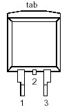
PHB20NQ20T: Features: • 'Trench' technology• Very low on-state resistance• Fast switching• Low thermal resistancePinoutSpecifications SYMBOL PARAMETER CONDITIONS MIN. MAX...
floor Price/Ceiling Price
- Part Number:
- PHB20NQ20T
- Supply Ability:
- 5000
Price Break
- Qty
- 1~5000
- Unit Price
- Negotiable
- Processing time
- 15 Days
SeekIC Buyer Protection PLUS - newly updated for 2013!
- Escrow Protection.
- Guaranteed refunds.
- Secure payments.
- Learn more >>
Month Sales
268 Transactions
Payment Methods
All payment methods are secure and covered by SeekIC Buyer Protection PLUS.

 PHB20NQ20T Data Sheet


