PHB101NQ03LT

Features: ·Low gate charge·Low on-state resistance.Application·Optimized as a control FET in DC to DC convertorsPinoutSpecifications Symbol Parameter Conditions Min Max Unit VDS drain-source voltage (DC) 25 Tj 175 - 30 V VDGR drain-gate voltage (DC) 25 Tj 175 ; RGS = ...

product image

PHB101NQ03LT Picture
SeekIC No. : 004460309 Detail

PHB101NQ03LT: Features: ·Low gate charge·Low on-state resistance.Application·Optimized as a control FET in DC to DC convertorsPinoutSpecifications Symbol Parameter Conditions Min Max Unit VDS drain-...

floor Price/Ceiling Price

Part Number:
PHB101NQ03LT
Supply Ability:
5000

Price Break

  • Qty
  • 1~5000
  • Unit Price
  • Negotiable
  • Processing time
  • 15 Days
Total Cost: $ 0.00

SeekIC Buyer Protection PLUS - newly updated for 2013!

  • Escrow Protection.
  • Guaranteed refunds.
  • Secure payments.
  • Learn more >>

Month Sales

268 Transactions

Rating

evaluate  (4.8 stars)

Upload time: 2024/12/30

Payment Methods

All payment methods are secure and covered by SeekIC Buyer Protection PLUS.

Notice: When you place an order, your payment is made to SeekIC and not to your seller. SeekIC only pays the seller after confirming you have received your order. We will also never share your payment details with your seller.
Product Details

Description


Features:

·Low gate charge
·Low on-state resistance.


Application

·Optimized as a control FET in DC to DC convertors


Pinout

  Connection Diagram


Specifications

Symbol Parameter Conditions Min Max Unit
VDS drain-source voltage (DC) 25 Tj 175 - 30 V
VDGR drain-gate voltage (DC) 25 Tj 175 ; RGS = 20 k - 30 V
VGS gate-source voltage (DC)   - ±20 V
VGSM gate-source voltage TP 50 s; pulsed; duty cycle = 25%;Tj 150   ±25  
ID drain current (DC) Tmb = 25 ; VGS = 10 V; Figure 2 and 3 - 75 A
Tmb = 100 ; VGS = 10 V; Figure 2 - 75 A
IDM peak drain current Tmb = 25 ; pulsed; tp 10 s; Figure 3 - 240 A
Ptot total power dissipation Tmb = 25 ; Figure 1 - 166 W
Tstg storage temperature   -55 +175
Tj junction temperature   -55 +175
Source-drain diode
IS source (diode forward) current (DC) Tmb = 25 - 74 A
ISM peak source (diode forward) current Tmb = 25 ; pulsed; tp 10 s - 240 A
Avalanche ruggedness
EDS(AL)S non-repetitive drain-source
avalanche energy
unclamped inductive load; ID = 43A;
tp = 0.19 ms; VDD 15 V; RGS = 50 ; VGS = 10 V; starting Tj = 25
- 185 mJ


Description

N-channel logic level field-effect power transistor in a plastic package using TrenchMOS™ technology.

Product availability:

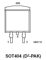
PHB101NQ03LT in SOT404 (D2-PAK)

PHD101NQ03LT in SOT428 (D-PAK).


Customers Who Bought This Item Also Bought

Margin,quality,low-cost products with low minimum orders. Secure your online payments with SeekIC Buyer Protection.
Power Supplies - External/Internal (Off-Board)
Discrete Semiconductor Products
Inductors, Coils, Chokes
Boxes, Enclosures, Racks
Fans, Thermal Management
View more