PBSS3515VS

Features: · 300 mW total power dissipation· Very small 1.6 x 1.2 mm ultra thin package· Self alignment during soldering due to straight leads· Low collector-emitter saturation voltage· High current capability· Improved thermal behaviour due to flat leads· Replaces two SC75/SC89 packaged low VCEsat...

product image

PBSS3515VS Picture
SeekIC No. : 004455627 Detail

PBSS3515VS: Features: · 300 mW total power dissipation· Very small 1.6 x 1.2 mm ultra thin package· Self alignment during soldering due to straight leads· Low collector-emitter saturation voltage· High current ...

floor Price/Ceiling Price

Part Number:
PBSS3515VS
Supply Ability:
5000

Price Break

  • Qty
  • 1~5000
  • Unit Price
  • Negotiable
  • Processing time
  • 15 Days
Total Cost: $ 0.00

SeekIC Buyer Protection PLUS - newly updated for 2013!

  • Escrow Protection.
  • Guaranteed refunds.
  • Secure payments.
  • Learn more >>

Month Sales

268 Transactions

Rating

evaluate  (4.8 stars)

Upload time: 2025/1/10

Payment Methods

All payment methods are secure and covered by SeekIC Buyer Protection PLUS.

Notice: When you place an order, your payment is made to SeekIC and not to your seller. SeekIC only pays the seller after confirming you have received your order. We will also never share your payment details with your seller.
Product Details

Description


Features:

· 300 mW total power dissipation
· Very small 1.6 x 1.2 mm ultra thin package
· Self alignment during soldering due to straight leads
· Low collector-emitter saturation voltage
· High current capability
· Improved thermal behaviour due to flat leads
· Replaces two SC75/SC89 packaged low VCEsat transistors on same PCB area
· Reduces required PCB area
· Reduced pick and place costs.


Application

· General purpose switching and muting
· Low frequency driver circuits
· LCD backlighting
· Audio frequency general purpose amplifier applications
· Battery driven equipment (mobile phones, video cameras and hand-held devices).


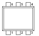
Pinout

  Connection Diagram


Specifications

SYMBOL PARAMETER CONDITIONS MIN. MAX. UNIT
Per transistor unless otherwise specified
VCBO collector-base voltage open emitter - -15 V
VCEO collector-emitter voltage open base - -15 V
VEBO emitter-base voltage open collector - -6 V
IC collector current (DC)   - -500 A
ICM peak collector current limited by Tj max - -1 A
IB base current (DC)   - -100 mA
Ptot total power dissipation Tamb 25 °C; note 1 - 200 mW
Tstg storage temperature   -65 +150 mW
Tj junction temperature   - 150 °C
Tamb operating ambient temperature   -65 +150 °C
Per device
Ptot total power dissipation Tamb 25 °C; note 2 - 300 °C
Note
1. Transistor mounted on an FR4 printed-circuit board.


Description

PNP low VCEsat double transistor PBSS3515VS in a SOT666 plastic package.

NPN complement: PBSS2515VS.


Customers Who Bought This Item Also Bought

Margin,quality,low-cost products with low minimum orders. Secure your online payments with SeekIC Buyer Protection.
Power Supplies - External/Internal (Off-Board)
Programmers, Development Systems
Soldering, Desoldering, Rework Products
Prototyping Products
DE1
RF and RFID
View more