PACE1753

Features: ` Implements the MIL-STD-1750A Instruction Set` ` Architecture for Memory Management and` Protection of up to 1 Megaword. All mapping` memory (10,240 bits) for both the MMU and` BPU functions are included on the chip.` Designed to interface memory to the` PACE1750A/AE 16-bit, 40 MHz proc...

product image

PACE1753 Picture
SeekIC No. : 004453930 Detail

PACE1753: Features: ` Implements the MIL-STD-1750A Instruction Set` ` Architecture for Memory Management and` Protection of up to 1 Megaword. All mapping` memory (10,240 bits) for both the MMU and` BPU functi...

floor Price/Ceiling Price

Part Number:
PACE1753
Supply Ability:
5000

Price Break

  • Qty
  • 1~5000
  • Unit Price
  • Negotiable
  • Processing time
  • 15 Days
Total Cost: $ 0.00

SeekIC Buyer Protection PLUS - newly updated for 2013!

  • Escrow Protection.
  • Guaranteed refunds.
  • Secure payments.
  • Learn more >>

Month Sales

268 Transactions

Rating

evaluate  (4.8 stars)

Upload time: 2024/11/25

Payment Methods

All payment methods are secure and covered by SeekIC Buyer Protection PLUS.

Notice: When you place an order, your payment is made to SeekIC and not to your seller. SeekIC only pays the seller after confirming you have received your order. We will also never share your payment details with your seller.
Product Details

Description


Features:

` Implements the MIL-STD-1750A Instruction Set
` ` Architecture for Memory Management and
` Protection of up to 1 Megaword. All mapping
` memory (10,240 bits) for both the MMU and
` BPU functions are included on the chip.
` Designed to interface memory to the
` PACE1750A/AE 16-bit, 40 MHz processor.
` Systems can be designed where no WAIT
` states are required up to 40 MHz clock rates
` when using these PACE products.
` System performance and device count are
` optimized when used with the PACE1754
` Processor Interface Circuit (PIC).
` Provides the following additional functions:
- EDAC, Error Detection and Correction-or
` parity generation and detection
- Correct data register-for diagnostics
- First memory failing address register
- Illegal address error detection-
` programmable
- Multi-Master arbitration
` 8-bit extended address latches and drivers on chip
` Information bus and EDAC transceivers on chip
` 20, 30 and 40 MHz operation over the Military
` Temperature Range
` Single 5V ± 10% Power Supply
` Power Dissipation over Military Temperature
` Range (PD Outputs Open)
< 0.20 watts at 20 MHz
< 0.30 watts at 30 MHz
< 0.40 watts at 40 MHz
` Available in:
- 64-Pin DIP or Gull Wing (50 Mil Pin centers)
- 68-Pin Pin Grid Array (PGA) (100 Mil centers)
- 68-Lead Quad Pack (Leaded Chip Carrier)


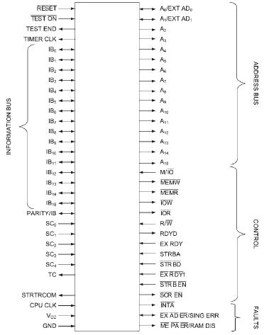
Pinout

  Connection Diagram


Specifications

Supply Voltage Range 0.5V to +7.0V
Input Voltage Range 0.5V to VCC + 0.5V
Storage Temperature Range 65°C to +150°C
Input Current Range 30mA to +5mA
Current applied to any output3 150mA
Maximum Power Dissipation2 1.5W
Lead Temperature Range
(soldering 10 seconds)
300°C
Thermal resistance (JC):4
Cases X and T
Cases Y and U
Case Z
8°C/W
5°C/W
6°C/W
Notes
1. Stresses above the absolute maximum rating may cause
permanent damage to the device. Extended operation at the
maximum levels may degrade performance and affect reliability.
2. Must withstand the added power dissipation due to short circuit
test e.g., IOS.
3. Duration 1 second or less.
4. Device Type Definitions from 5962-89505 SMD:
Case X: Dual In-Line
Case T: Dual In-Line with Gull-Wing Leads
Case Y: Leaded Chip Carrier with Gull-Wing Leads
Case U: Leaded Chip Carrier with Unformed Leads
Case Z: Pin Grid Array


Description

The PACE1753 (COMBO) is a support chip for the PACE1750A/AE microprocessor family. It provides the following supporting functions to the system:

1. Memory management and access protection for up to 1M words.

2 Physical memory write protection for up to 1M words memory in pages of 1K words each. Separate protection is provided for the CPU and for DMA in systems which include DMA.

3. Detection of illegal l/O accesses (as defined by MILSTD- 1750A) or access to an unimplemented block of memory. In each case an error flag is generated to the processor.

4 Detection of double errors on the data bus and correction of single errors. An error signal is generated to the processor when a multiple error is detected.

5. RDYA generation. Up to three wait states can be inserted in the address phase of the bus by generating a not-ready, RDYA low signal. The number of wait states required can be programmed in an internal register in the COMBO.

6. Bus arbitration for up to 4 masters. Arbitration is done on a fixed priority basis (i.e. by interconnection of hardware). (In 68 pin package only).


Customers Who Bought This Item Also Bought

Margin,quality,low-cost products with low minimum orders. Secure your online payments with SeekIC Buyer Protection.
RF and RFID
Cables, Wires - Management
Industrial Controls, Meters
Optoelectronics
Hardware, Fasteners, Accessories
View more