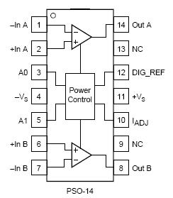
Features: ` WIDEBAND ±12V OPERATION: 25MHz (G = +8)
` UNITY GAIN STABLE: 35MHz (G = +1)
` HIGH OUTPUT CURRENT: 250mA
` OUTPUT VOLTAGE SWING: ±10.5V (VS = ±12V)
` HIGH SLEW RATE: 600V/s
` LOW SUPPLY CURRENT: 8mA/channel
`l FLEXIBLE POWER CONTROL (SO-14)
` ±6V TO ±16V SUPPLY RANGE
` POWER PACKAGINGApplication· xDSL LINE DRIVER
· LOW-NOISE ADSL RECEIVER
· LOW-COST VIDEO DA
· LOW-COST UPGRADE TO LT1207/AD812Pinout Specifications
Power Supply ........................................... ±16.5VDC
Internal Power Dissipation(1) ............ See Thermal Information
Differential Input Voltage .................................. ±5V
Input Voltage Range ......................................... ±VS
Storage Temperature Range: U, N ............... 40°C to +125°C
Lead Temperature (soldering, 10s) ........................ +260°C
Junction Temperature (TJ ) ............................... +175°C
ESD Rating (Human Body Model) .............................. 4000V
(Machine Model) ..............................................300V |
NOTE:: (1) Packages must be derated based on specified A. Maximum TJ
must be observed.DescriptionThe OPA2607 provides a high output voltage swing and low distortion required for low turns ratio ADSL upstream driver applications. Operating on a ±12V supply, the OPA2607 consumes a low 8.0mA/channel quiescent current to deliver a very high 250mA peak output current. Guaranteed output current of 180mA supports even the most demanding ADSL CPE requirements with low harmonic distortion. Differential driver applications will deliver < 75dBc distortion at the peak upstream power levels of full rate ADSL. Using a differential driver design, as shown below, the OPA2607 can deliver a high 38Vp-p voltage swing into a 1:0.8 step-down transformer to meet the ADSL CPE upstream power requirements. This low turns ratio actually provides a step up to the much weaker downstream signal arriving on the line side of this transformer, extending the DSL modem's reach.
OPA2607 Power control features are included in the SO-14 package version to allow system power to be minimized. Two logic control lines allow four quiescent power settings. These include full power, power cutback for short loops, idle state for no signal transmission but line match maintenance, and shutdown for power off with a high impedance output. An additional I
ADJ pin allows the maximum supply current to be adjusted ±25% from the nominal value. Connecting this pin to +V
CC will increase the full power quiescent to 20mA, increasing the peak output current available, while connecting this pin to V
CC will decrease the full power quiescent to 12mA where a lower peak output current is required. The digital control lines continue to scale the total quiescent current from these new maximum levels in the same proportional steps as before.
The OPA2607 is available in three package styles. For power driver applications, a thermally enhanced package with a heat slug is available in both SO-8 and SO-14 pinouts. For lower power receiver applications, a standard SO-8 package is available.

 OPA2607 Data Sheet


