Radiant Intensity
:
Package / Case
:
Maximum Operating Temperature
: + 85 C
Minimum Operating Temperature
: - 40 C
Packaging
: Bulk
Wavelength
: 890 nm
Beam Angle
: 25 deg
Features: `Very Low Noise 5 nV/Hz @ 1 kHz Max
`Excellent Input Offset Voltage 75 V Max
`Low Offset Voltage Drift 1 V/0C Max
`Very High Gain 1500 V/mV Min
`Outstanding CMR 106 dB Min
`Slew Rate 2.4 V/s Typ
`Gain Bandwidth Product 5 MHz Typ
`Industry-Standard 8-Lead Dual PinoutPinout Specifications
Supply Voltage . . . . . . . . . . . . . . . . . . . . . . . . . . . . . . ±18 V
Differential Input Voltage2 . . . . . . . . . . . . . . . . . . . . . ±1.0 V
Differential Input Current2 . . . . . . . . . . . . . . . . . . . . ±25 mA
Input Voltage . . . . . . . . . . . . . . . . . . . . . . . . Supply Voltage
Output Short-Circuit Duration . . . . . . . . . . . . . . . Continuous
Storage Temperature Range
P, S, Z Package . . . . . . . . . . . . . . . . . . . 65°C to +150°C
Lead Temperature Range (Soldering, 60 sec) . . . .. . . 300°C
Junction Temperature (TJ) . . . . . . . . . . . .65°C to +150°C
Operating Temperature Range
OP270E, OP270F, OP270G . . . . . . . . .. . . . 40°C to +85°C
NOTES
1 Stresses above those listed under Absolute Maximum Ratings may cause permanent damage to the device. This is a stress rating only; functional operation of the device at these or any other conditions above those listed in the operational sections of this specification is not implied. Exposure to absolute maximum rating conditions for extended periods may affect device reliability.
2 The OP270's inputs are protected by back-to-back diodes. Current limiting resistors are not used, in order to achieve low noise performance. If differential voltage exceeds +10 V, the input current should be limited to ±25 mA.
| -3dB Bandwidth |
5MHz |
| Slew Rate |
2.4V/s |
| Vos |
50V |
| Ib |
15nA |
| Input Noise (nV/rtHz) |
3.2nV/rtHz |
| Vcc-Vee Supply (V) |
9 to 36 |
| Iq per Amplifier (max) |
3.25mA |
| # OpAmps per Pkg |
2 |
| Operating Temp Range |
-55 to +125 |
| Packages |
DIP,SOIC |
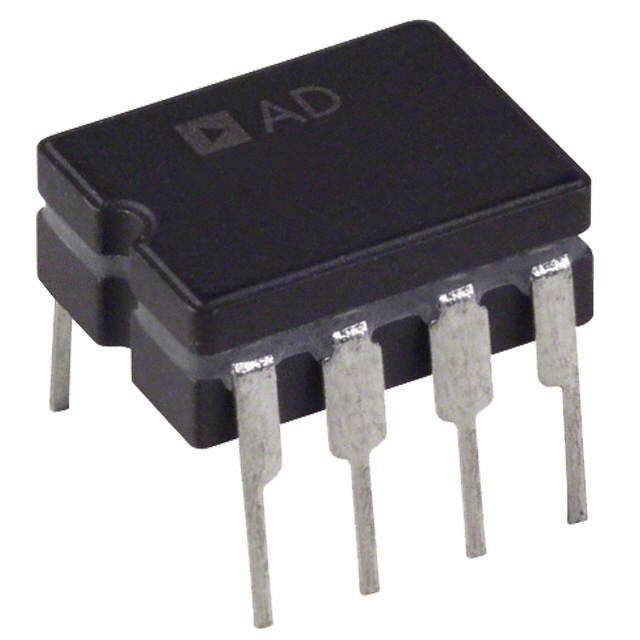
DescriptionThe OP270 is a high performance, monolithic, dual operational amplifier with exceptionally low voltage noise, 5 nV/Hz max at 1 kHz. It offers comparable performance to ADI's industry standard OP27.
The OP270 features an input offset voltage below 75 mV and an offset drift under 1 V/0C, guaranteed over the full military temperature range. Open-loop gain of the OP270 is over 1,500,000 into a 10 k load, ensuring excellent gain accuracy and linearity, even in high gain applications. Input bias current is under 20 nA, which reduces errors due to signal source resistance. The OP270's CMR of over 106 dB and PSRR of less than 3.2 mV/V significantly reduce errors due to ground noise and power supply fluctuations. Power consumption of the dual OP270 is one-third less than two OP27s, a significant advantage for power conscious applications. The OP270 is unity-gain stable with a gain bandwidth product of 5 MHz and a slew rate of 2.4 V/s.
The OP270 offers excellent amplifier matching, which is important for applications such as multiple gain blocks, low noise instrumentation amplifiers, dual buffers, and low noise active filters.
The OP270 conforms to the industry-standard 8-lead DIP pinout. It is pin compatible with the MC1458, SE5532/A, RM4558, and HA5102 dual op amps, and can be used to upgrade systems using those devices.
For higher speed applications, the OP271, with a slew rate of 8 V/s, is recommended. For a quad op amp, see the OP470.
Parameters: | Technical/Catalog Information | OP270 |
| Vendor | TT Electronics/Optek Technology |
| Category | Optoelectronics |
| Voltage - Forward (Vf) Typ | 1.5V |
| Current - DC Forward (If) | 50mA |
| Wavelength | 890nm |
| Viewing Angle | 25° |
| Radiant Intensity (Ie) Min @ If | - |
| Mounting Type | Surface Mount |
| Package / Case | Non-Standard SMD |
| Orientation | Top View |
| Packaging | - |
| Lead Free Status | Lead Free |
| RoHS Status | RoHS Compliant |
| Other Names | OP270
OP270
365 1150 ND
3651150ND
365-1150
|

 OP270 Data Sheet


