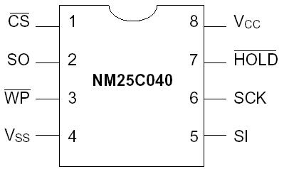
Features: ·2.1 MHz clock rate @ 2.7V to 5.5V·4096 bits organized as 512 x 8·Multiple chips on the same 3-wire bus with separate chip select lines·Self-timed programming cycle·Simultaneous programming of 1 to 4 bytes at a time·Status register can be polled during programming to monitor READY/BUSY·W...
NM25C040: Features: ·2.1 MHz clock rate @ 2.7V to 5.5V·4096 bits organized as 512 x 8·Multiple chips on the same 3-wire bus with separate chip select lines·Self-timed programming cycle·Simultaneous programmin...
SeekIC Buyer Protection PLUS - newly updated for 2013!
268 Transactions
All payment methods are secure and covered by SeekIC Buyer Protection PLUS.
The NM25C040 is a 4096-bit CMOS EEPROM with an SPI compatible serial interface. The NM25C040 is designed for data storage in applications requiring both non-volatile memory and insystem data updates. This EEPROM is well suited for applications using the 68HC11 series of microcontrollers that support the SPI interface for high speed communication with peripheral devices via a serial bus to reduce pin count. The NM25C040 is implemented in Fairchild Semiconductor's floating gate CMOS process that provides superior endurance and data retention.
The serial data transmission of NM25C040 requires four signal lines to control the device operation: Chip Select (CS), Clock (SCK), Data In (SI), and Serial Data Out (SO). All programming cycles are completely self-timed and do not require an erase before WRITE.
BLOCK WRITE protection of NM25C040 is provided by programming the STATUS REGISTER with one of four levels of write protection. Additionally, separate WRITE enable and WRITE disable instructions are provided for data protection.
Hardware data protection of NM25C040 is provided by the WP pin to protect against inadvertent programming. The HOLD pin allows the serial communication to be suspended without resetting the serial sequence.