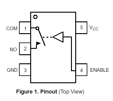
Features: • Guaranteed RON of 32 at 5.5 V• Low Power Dissipation: ICC = 2 A• Low Threshold Enable pin TTL compatible at 5.0 Volts• TTL version and pin for pin with NLAS4501• Provides Voltage translation for many different voltage levels 3.3 to 5.0 Volts, Enable pin m...
NLAST4501: Features: • Guaranteed RON of 32 at 5.5 V• Low Power Dissipation: ICC = 2 A• Low Threshold Enable pin TTL compatible at 5.0 Volts• TTL version and pin for pin with NLAS4501&...
SeekIC Buyer Protection PLUS - newly updated for 2013!
268 Transactions
All payment methods are secure and covered by SeekIC Buyer Protection PLUS.
US $.2 - .23 / Piece
Multiplexer Switch ICs 2:1 Mux/Demux Switch -55 to 125deg C
• Guaranteed RON of 32 at 5.5 V
• Low Power Dissipation: ICC = 2 A
• Low Threshold Enable pin TTL compatible at 5.0 Volts
• TTL version and pin for pin with NLAS4501
• Provides Voltage translation for many different voltage levels 3.3 to 5.0 Volts, Enable pin may go as high as 5.5 Volts 1.8 to 3.3 Volts 1.8 to 2.5 Volts
• Improved version of MAX4501 (at any voltage between 2 and 5.5 Volts)
• Chip Complexity: FETs = 11
Symbol | Parameter | Value | Unit |
VCC | Positive DC Supply Voltage | -0.5 to +7.0 | V |
VIS | Analog Input Voltage (VNO or VCOM) | -0.5 to +7.0 | V |
VIN | Digital Select Input Voltage | -0.5 to VCC +0.5 | V |
IIK | DC Current, Into or Out of Any Pin | ±20 | mA |
TSTG | Storage Temperature Range | -65 to +150 | |
TL | Lead Temperature, 1 mm from Case for 10 Seconds | 260 | |
TJ | Junction Temperature under Bias | +150 | |
JA | Thermal Resistance SC70−5/SC−88A (Note 1) TSOP−5 |
350 230 |
°C/W |
PD | Power Dissipation in Still Air at 85°C SC70−5/SC−88A TSOP−5 |
150 200 |
mW |
MSL | Moisture Sensitivity | Level 1 | |
FR | Flammability Rating Oxygen Index: 28 to 34 | UL 94−V0 (0.125 in) | |
VESD | ESD Withstand Voltage Human Body Model (Note 1) Machine Model (Note 2) Charged Device Model (Note 3) |
> 2000 > 100 N/A |
V |
ILatchUp | LatchUp Performance Above VCC and Below GND at 85 (Note 5) | ±300 | mA |
Maximum Ratings are those values beyond which damage to the device may occur. Exposure to these conditions or conditions beyond those indicated may adversely affect device reliability. Functional operation under absolute−maximum−rated conditions is not implied. Functional operation should be restricted to the Recommended Operating Conditions.
1. Measured with minimum pad spacing on an FR4 board, using 10 mm−by−1 inch, 2−ounce copper trace with no air flow.
2. Tested to EIA/JESD22−A114−A.
3. Tested to EIA/JESD22−A115−A.
4. Tested to JESD22−C101−A.
5. Tested to EIA/JESD78.
The NLAST4501 is an analog switch manufactured in sub−micron silicon−gate CMOS technology. NLAST4501 achieves very low RON while maintaining extremely low power dissipation. NLAST4501 is a bilateral switch suitable for switching either analog or digital signals, which may vary from zero to full supply voltage.
The NLAST4501 is a low voltage, TTL (low threshold) compatible device, pin for pin compatible with the MAX4501.
The Enable pin of NLAST4501 is compatible with standard TTL level outputs when supply voltage is nominal 5.0 Volts. It is also over−voltage tolerant, making it a very useful logic level translator.